Solid state light emitter package, a lamp, a luminaire and a method of manufacturing a solid state light emitter package

Active Publication Date: 2020-01-30
SIGNIFY HLDG BV
View PDF0 Cites 0 Cited by
  • Summary
  • Abstract
  • Description
  • Claims
  • Application Information

AI Technical Summary

Benefits of technology

[0011]The solid state light emitter package or the manufactured solid state light emitter package are more safe then known solid state light emitter packages because the risk of carbonizing of all electrical insulating material isolators is reduced. If one of the lead frames is becoming relatively hot, for example, because of a relatively high ohmic contact between one of the lead frames and an element that is electrically connected to the lead frame, then the heat is absorbed or spread by the thermal element before the heat is capable of fully carbonizing the whole structure in between the first lead frame and the thermal element and in between the thermal element and the second lead frame. Thereby the risk of a short circuit and, thus, a burning solid state light emitter package is reduced. Additionally, the thermal element is an additional element in between the first lead frame and the second lead frame and the thermal element is electrically isolated from the first lead frame and the second lead frame and, thus it has a floating voltage (assuming that it is partially electrical conductive). Thereby a gap between the first lead frame and the second lead frame is larger and, thus, a higher voltage difference between the first lead frame and the second lead frame is needed before a short circuit between them can occur. In other words, the increased distance also contributes to a lower risk of a short circuit and, thus, a burning solid state light emitter package.
[0012]If the thermal element is a heat absorber it is clear that more heat must be generated before this is all transferred through all the materials that are in between the first lead frame and the second lead frame and that, thereby, the risk of carbonization along a shortest path between the first lead frame and the second lead frame is reduced and at least delayed. Often a high ohmic connection is located in a relatively small area and, thus, the heat is generated in a relatively small area. Along the shortest thermal path to an opposing lead frame the electrical insulator can carbonize because of the very high local temperatures. The shortest thermal path from this relatively small area towards an opposing lead frame can be interrupted by a heat spreader. The heat spreader bet

Problems solved by technology

A problem with such a light-emitting-element mount substrate is that, for example, the connection of the LED to one of the substrate bodies becomes high ohmic as the result of, for example, corrosion or damage as the result of, for example, an electrostatic discharge (

Method used


Image

  • Solid state light emitter package, a lamp, a luminaire and a method of manufacturing a solid state light emitter package
  • Solid state light emitter package, a lamp, a luminaire and a method of manufacturing a solid state light emitter package
  • Solid state light emitter package, a lamp, a luminaire and a method of manufacturing a solid state light emitter package

Examples


first embodiment

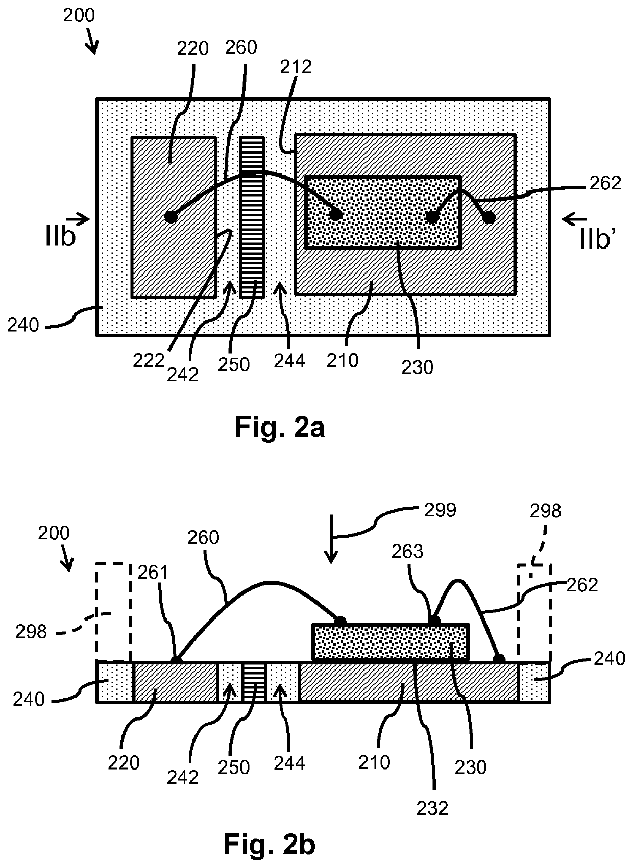
[0040]FIG. 2a schematically shows a top view of a solid state light emitter package 200 according to an aspect of the invention. The solid state light emitter package comprises a solid state light emitter die 230, a first lead frame 210, a second lead frame 220, an electrical insulating material 242, 244 (being formed by material of a support element 240 of the solid state light emitter package 200), a thermal element 250, and a second bonding wire 260. Optionally, a first bonding wire 262 is provided.

[0041]The top view is along a view direction towards a side of the first lead frame 210 on which the solid state light emitter die 230 is provided. In FIG. 2b an arrow 299 is drawn that indicates the viewing direction along which the top view of FIG. 2a is obtained. In subsequent embodiments, the top view is obtained along an equal or similar viewing direction.

[0042]The solid state light emitter die 230 may be a Light Emitting Diode (LED) die, but may also be another type of solid stat...

second embodiment

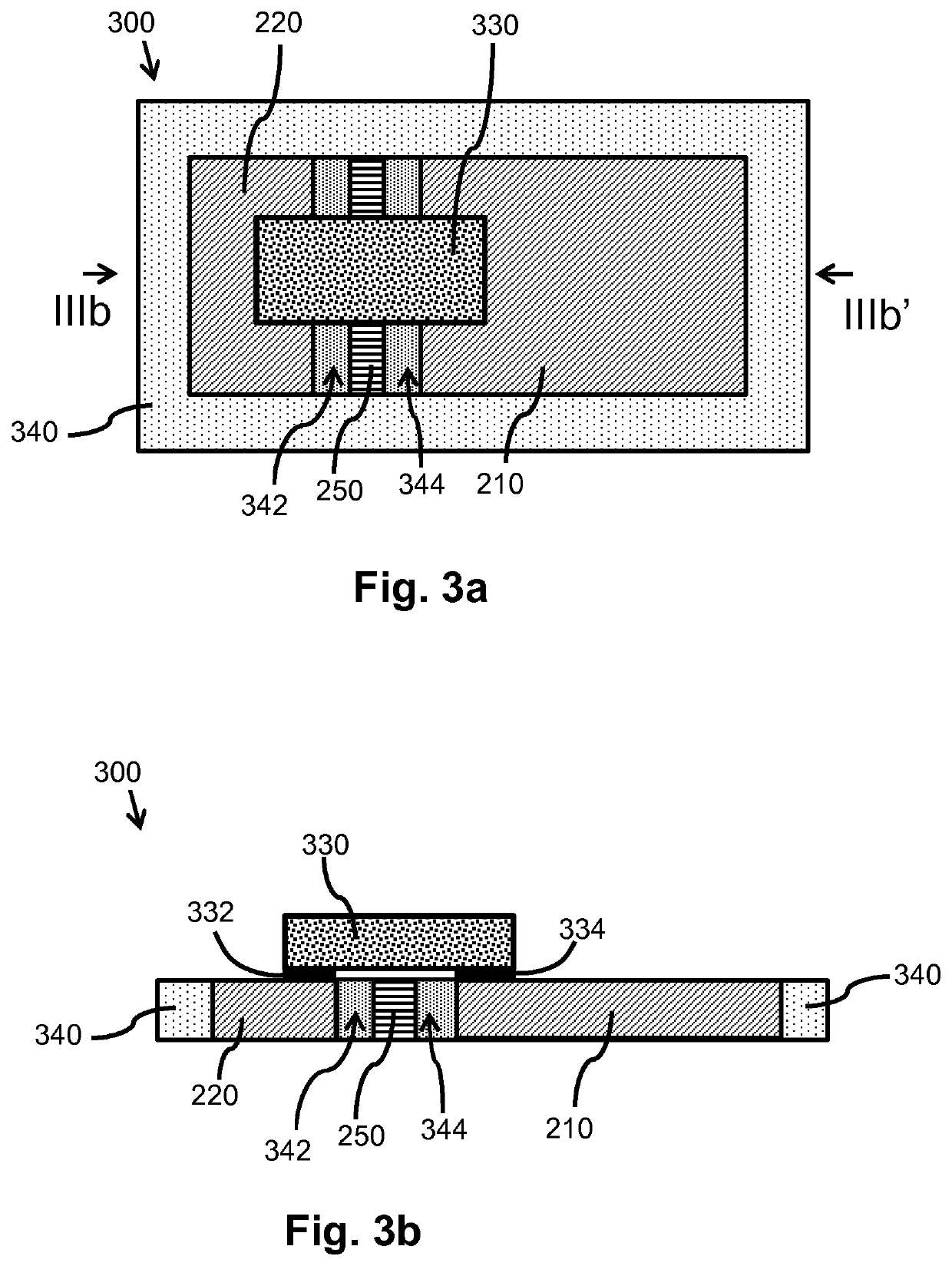
[0060]Also in the context of the solid state light emitter package 300 it is advantageous to have the thermal element 250 in between the lead frames 210, 220. In the context of FIGS. 3a, 3b one of the coupling between the solid state light emitter die 330 and one of the lead frames 210, 220 may be high-ohmic and may, consequently, dissipate quite some power in the coupling alone. Thereby the one of the lead frames may become too hot and one of the electrically insulating materials 342, 344 may carbonize. The thermal element 250 will prevent, or at least will delay, that the other one of the electrically insulating materials 342, 344 carbonizes as well. Thereby the solid state light emitter package 300 is safer.

[0061]FIG. 4a schematically shows a top view of a third embodiment of a solid state light emitter package 400. Solid state light emitter package 400 is similar to solid state light emitter package 200 and may have similar embodiments that have similar effects and advantages as...

fifth embodiment

[0066]FIG. 5a schematically shows a top view of a solid state light emitter package 500. Solid state light emitter package 500 is similar to solid state light emitter package 200 and may have similar embodiments that have similar effects and advantages as discussed in the context of FIG. 2a. Differences are discussed hereinafter and a discussion of the elements that are similar or equal is provided in the context of FIG. 2a. Features of other embodiments of the solid state light emitter package 300, 400, 450 of FIGS. 3a, 3b, 4a and 4b may also be combined with the presented embodiment.

[0067]In the solid state light emitter package 500, the second lead frame 520 is relatively small and provided inside a U-shaped thermal element 548. In between the U-shaped thermal element 548 and the second lead frame 520 is provided an electrically insulating material 542. In between the thermal element 548 and the first lead frame 210 is also provided an electrically insulating material 544. The th...


PUM


Abstract

A solid state light emitter package (200), a lamp, a luminaire and a method of manufacturing the solid state light emitter package are provided. The solid state light emitter package comprising a solid state light emitter die (230), a first and second lead frame (210, 220), an electrical insulating material (242, 244), a thermal element (250) and a bridging element (260). The first and second lead frame are electrically isolated from each other and provide power to said die. Said die is at least partially provided on the first lead frame. The thermal element is in between the first and second lead frame and is electrically isolated by the electrical insulating material from said lead frames. The thermal element is at least one of a heat absorber or a heat spreader. The bridging element bridges the electrical insulating material and the thermal element and provides an electrical connection between said die and the second lead frame.

Description

FIELD OF THE INVENTION[0001]The invention relates to a solid state light emitter package. The invention further relates to a lamp and to a luminaire comprising an embodiment of the solid state light emitter package.[0002]The invention also relates to a method of manufacturing a solid state light emitter package.BACKGROUND OF THE INVENTION[0003]Light Emitting diode (LED) dies are often packaged in a LED package before being used in a lighting application. During the lifetime of the LED die and LED package it may be that, at a certain point in time, elements of the LED package become too hot, that these or other elements of the LED package may carbonize under the influence of the heat, and as a consequence of a short circuit the LED package may catch fire. There is a strong need to prevent this and manufacture LED packages that are safe, even in cases of overheating.[0004]U.S. Pat. No. 9,240,535B2 describes a light-emitting-element mount substrate that should have good heat release pr...

Claims


Application Information

Patent Timeline
IPC IPC(8): H01L33/64H01L33/62H01L33/48H01L23/00
CPCH01L2933/0066H01L33/641H01L33/62H01L33/644H01L2224/48245H01L33/642H01L24/48H01L2933/0075H01L24/16H01L2224/16245H01L33/483H01L33/486H01L2224/48091H01L2924/00014H01L23/49537H01L23/49541H01L23/49575
Inventor JACOBS, BOUDEWIJNVAN DRIEL, WILLEM DIRKVAN DER MAREL, CORNELIS
Owner SIGNIFY HLDG BV
Why Eureka
Try Eureka