Eureka AIR delivers breakthrough ideas for toughest innovation challenges, trusted by R&D personnel around the world.

Amplifier

Active Publication Date: 2020-01-30
NIPPON TELEGRAPH & TELEPHONE CORP
View PDF0 Cites 1 Cited by
  • Summary
  • Abstract
  • Description
  • Claims
  • Application Information

AI Technical Summary

Benefits of technology

The present invention provides an amplifier for the TIA that reduces the noise caused by the current source. This improves the quality of the signal being transmitted.

Problems solved by technology

However, in the case where the amplifier includes therein a current source, the current source causes high noise, which disadvantageously causes a deteriorated noise characteristic of the TIA.
In the case of the above-described TIA in which the current source is connected to the input terminal in particular, noise has an influence on a stage prior to the amplification of the input signal, thus causing a very-remarkable deterioration of the noise characteristic.

Method used


Image

  • Amplifier
  • Amplifier
  • Amplifier

Examples


first embodiment

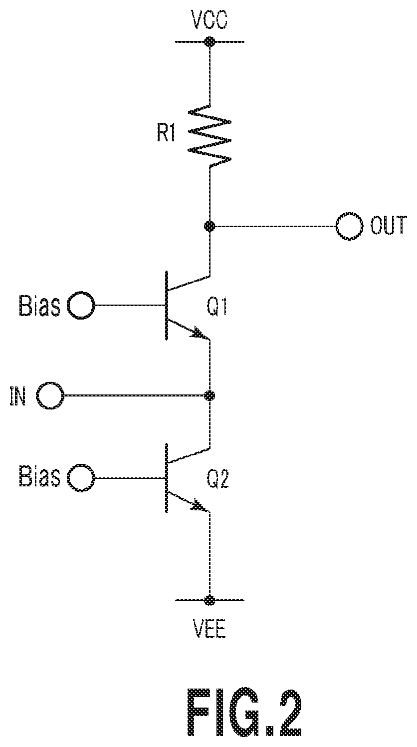
[0041]FIG. 6 illustrates the configuration of the grounded base-type TIA according to the present invention. The grounded base-type TIA includes the transistor Q2 and an inductor L1 serially inserted between the input terminal IN and the negative-side power source voltage VEE and an amplification stage consisting of the transistor Q1 and the resistance R1. The transistor Q2 has a base terminal that is connected to a current control bias to control the DC current flowing in the transistor Q1 and the DC component of the input signal current. The emitter terminal of the transistor Q2 is connected to the inductor element to thereby configure a current source having a high internal impedance, thus suppressing the deterioration of the noise characteristic of the TIA due to the current source.

[0042]FIG. 7 illustrates the configuration of the grounded base-type TIA according to the second embodiment of the present invention. Between an emitter terminal of the transistor Q2 functioning as a ...

third embodiment

[0044]FIG. 8 illustrates the configuration of the grounded base-type TIA according to the present invention. A capacitive element C is connected in parallel to the inductor L1 at the grounded base-type TIA shown in FIG. 7. By the addition of the capacitive element C, the impedance Z seen from the emitter terminal of Q2 constituting the current source in the direction VEE can be calculated by the following formula.

Z=R2+jωL1-ω2LCFormula3ω2LC=1Formula4

second embodiment

[0045]At a frequency at which the Formula 4 is established, i.e., at a resonance point of the resonance circuit, |Z|=∞ is established. When compared with the second embodiment, a current source can be realized that has a higher internal impedance.

[0046]In an actual case, a resistance component parasitic in the inductor L1 for example prevents the impedance seen from the emitter terminal in the direction VEE from increasing to ∞. However, the impedance can be made to be seemingly high in the vicinity of the resonance point. The third embodiment is effectively applied to a case where the amplifier cannot include therein an inductor having a sufficiently-high inductance. Furthermore, an LC resonance point designed in the frequency band of the TIA can provide a particularly-high internal impedance.

[0047]FIGS. 9A and 9B illustrate a resonance circuit formed in the TIA chip. FIG. 9A is a bird's-eye view illustrating the inductor element having a three-dimensional structure formed in the T...


PUM


Abstract

An amplifier applied to TIA is provided to suppress the noise caused by a current source. An amplifier constituting a transimpedance amplifier includes an inductor element inserted between a current source connected to an input terminal of an amplification stage and a power source voltage line. The current source includes a first transistor in which a base terminal is connected to a current control bias and a collector terminal is connected to the input terminal. The inductor element is inserted between the emitter terminal of the first transistor and the power source voltage line.

Description

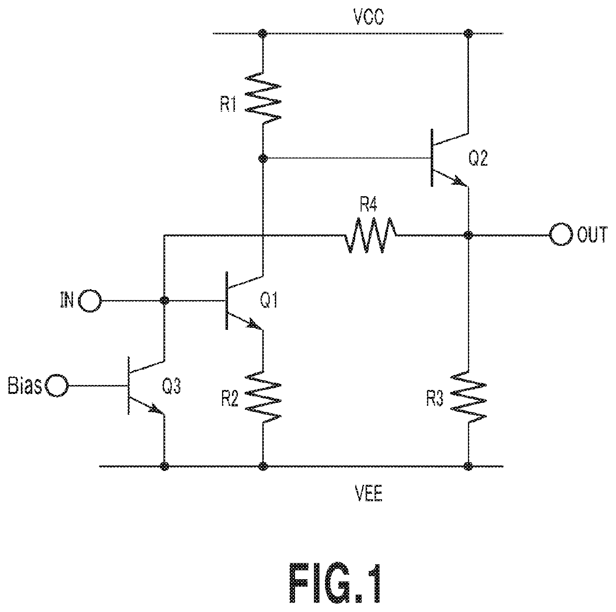
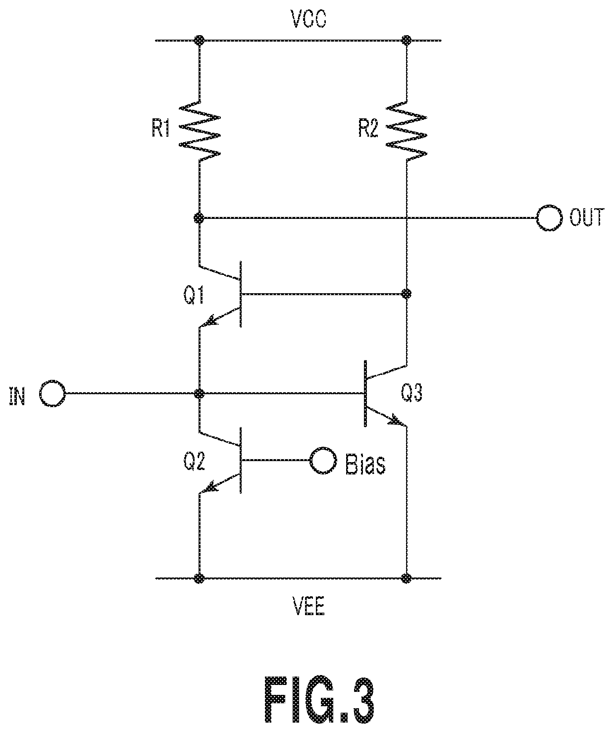
TECHNICAL FIELD[0001]The present invention relates to an amplifier. More particularly, the invention relates to an amplifier applied to a transimpedance amplifier to covert a current signal converted from an optical signal by a photodetector in an optical receiver to a voltage signal.BACKGROUND ART[0002]A transimpedance amplifier (TIA) is used for an optical receiver and amplifies the signal strength while converting a current signal converted from an optical signal by a photodetector to a voltage signal. The optical receiver is desired to be able to receive a minute optical signal. Thus, the TIA is desired to have a low noise characteristic.[0003]FIG. 1 illustrates the configuration of a conventional grounded emitter-type TIA. The grounded emitter-type TIA includes: a transistor Q3 inserted between an input terminal IN and a negative-side power source voltage VEE; an amplification stage consisting of a transistor Q1 and resistances R1 and R2; an output stage consisting of a transis...

Claims


Application Information

Patent Timeline
IPC IPC(8): H03F1/26H03F1/08H03F3/08H03F3/21H03F3/347H04B10/69
CPCH03F1/083H04B10/693H03F3/08H03F3/211H03F3/347H03F1/26H03F2200/294H03F2200/72
Inventor NAKANO, SHINSUKEKATSURAI, HIROAKINOGAWA, MASAFUMIKIMURA, SHUNJITOBAYASHI, MASATOSHIKURITA, SHIGEHIROENDO, MASAHIRO
Owner NIPPON TELEGRAPH & TELEPHONE CORP
Why Eureka
Eureka Blog
Learn More