Method for manufacturing semiconductor device and semiconductor device using the same

a semiconductor device and manufacturing method technology, applied in the direction of coatings, transistors, chemical vapor deposition coatings, etc., can solve the problems achieve the effect of shortening process time and process cost, improving uniformity of insulation layer formed by atomic layer deposition on semiconductor layer, and increasing precursor injection pressur

Active Publication Date: 2020-02-20
SAMSUNG DISPLAY CO LTD +1
View PDF5 Cites 0 Cited by
  • Summary
  • Abstract
  • Description
  • Claims
  • Application Information

AI Technical Summary

Benefits of technology

[0026]According to a method for manufacturing a semiconductor device according to the present disclosure, uniformity of an insulation layer formed by atomic layer deposition on a semiconductor layer can be

Problems solved by technology

In addition, it is possible to uniformly deposit the insulation layer

Method used


Image

  • Method for manufacturing semiconductor device and semiconductor device using the same
  • Method for manufacturing semiconductor device and semiconductor device using the same
  • Method for manufacturing semiconductor device and semiconductor device using the same

Examples


Embodiment Construction

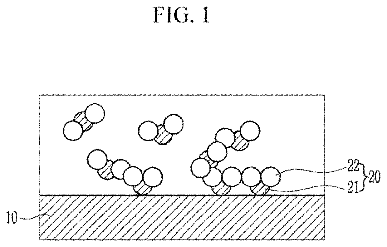
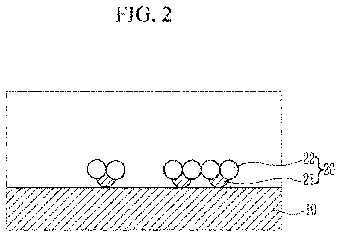
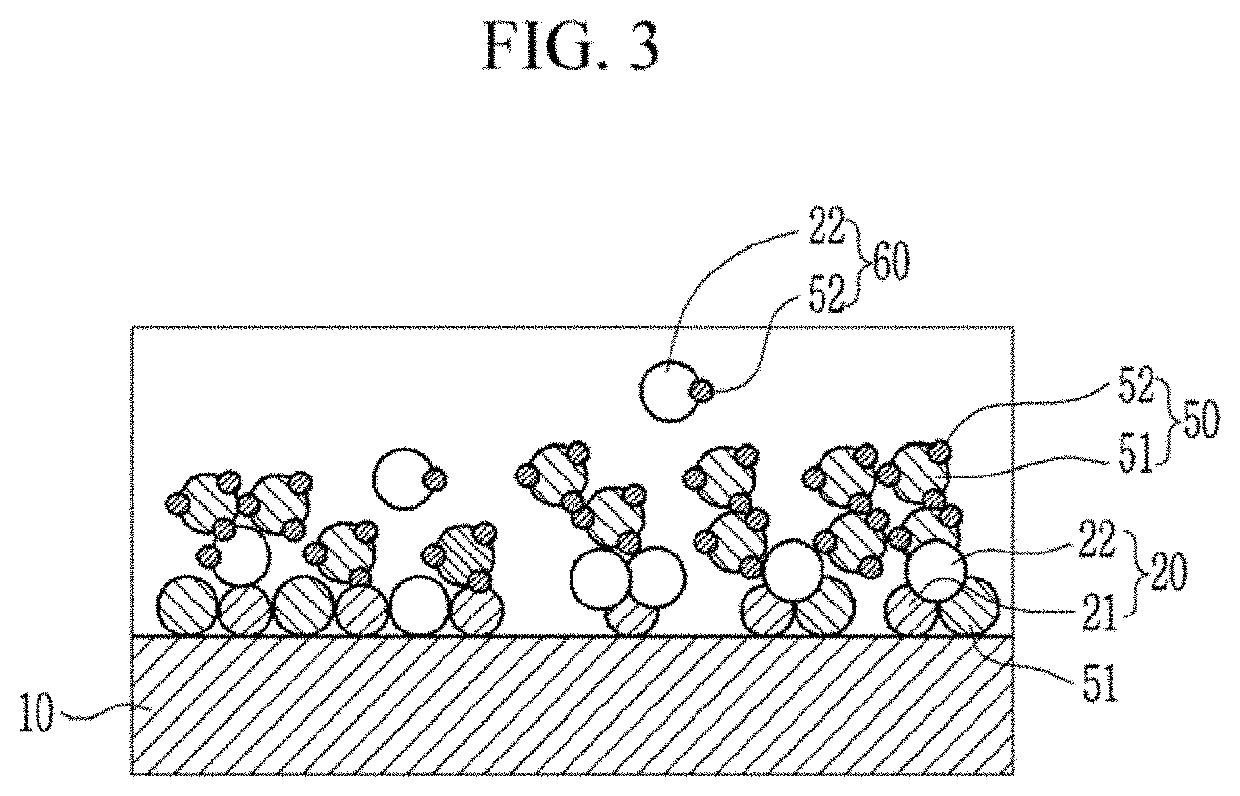
[0032]Embodiments of present disclosure will be described more fully hereinafter with reference to the accompanying drawings, in which exemplary embodiments of the disclosure are shown. As those skilled in the art would realize, exemplary embodiments may be modified in various different ways, all without departing from the spirit or scope of the present disclosure.

[0033]The drawings and description are to be regarded as illustrative in nature and not restrictive. Like reference numerals may designate like elements throughout the specification.

[0034]Since the size and the thickness of each configuration shown in the drawings are arbitrarily indicated for better understanding and ease of description, the present disclosure is not limited to as shown in the drawings, and the thickness of layers, films, panels, regions, etc., may be exaggerated for clarity.

[0035]It will lie understood that when an element such as a layer, film, region, or substrate is referred to as being “on” another e...


PUM

PropertyMeasurementUnit
Thicknessaaaaaaaaaa
Thicknessaaaaaaaaaa
Thicknessaaaaaaaaaa

Abstract

A method for manufacturing a semiconductor device according to an, exemplary embodiment of the present disclosure includes: forming a semiconductor layer on a substrate in a chamber; and forming a semiconductor layer on a substrate in a chamber. Forming the insulation layer includes: (a) injecting precursors that include a metal into a surface of the semiconductor layer; (b) removing precursors that are not adsorbed; (c) injecting reactants onto the surface of the semiconductor layer; and (d) removing residual reactants. The semiconductor layer includes a semiconductor material that has a layered structure.

Description

CROSS-REFERENCE TO RELATED APPLICATION[0001]This application claims priority under 35 U.S.C. § 119 from, and the benefit of, Korean Patent Application No. 10-2018-0096142, filed in the Korean Intellectual Property Office on Aug. 17, 2018, the contents of which are herein incorporated by reference in their entirety.BACKGROUNDTechnical Field[0002]Embodiments of the present disclosure are directed to a method for manufacturing a semiconductor device and a semiconductor device using the same, and more particularly, to a method for manufacturing a semiconductor device that forms a uniform insulation layer on a semiconductor layer by using an atomic layer deposition (ALD) method, and a semiconductor device manufactured therefrom.Discussion of the Related Art[0003]A semiconductor material that has a layered structure is flexible and transparent, and is thus attracting attention as a next-generation semiconductor material. In this case, a thin film, such as an insulation layer, is uniformly...

Claims


Application Information

Patent Timeline
IPC IPC(8): H01L21/02H01L29/66H01L29/49
CPCH01L21/02205H01L21/02274H01L21/0228H01L29/786H01L29/66045H01L29/4908H01L29/1606H01L29/24H01L29/78648H01L29/66969H01L21/02178H01L21/02175C23C16/45525H01L21/02172H01L21/02225H01L21/02568H01L21/28568
Inventor LIM, JUN HYUNGKIM, HYUNG JUNLEE, SUN HEESEO, SEUNG GIWOO, WHANG JE
Owner SAMSUNG DISPLAY CO LTD
Why Eureka
Try Eureka