

Multilayer ceramic electronic component and method of manufacturing the same
a multi-layer ceramic and electronic component technology, applied in the direction of capacitor manufacturing, fixed capacitor details, printed circuit non-printed electric components association, etc., can solve the problems of easy breaking of multi-layer ceramic capacitors, difficult thinning of elements, and difficulty in low profile, so as to achieve the effect of easy manufacturing
- Summary
- Abstract
- Description
- Claims
- Application Information
AI Technical Summary
Benefits of technology
Problems solved by technology
Method used
Image

Examples
first embodiment
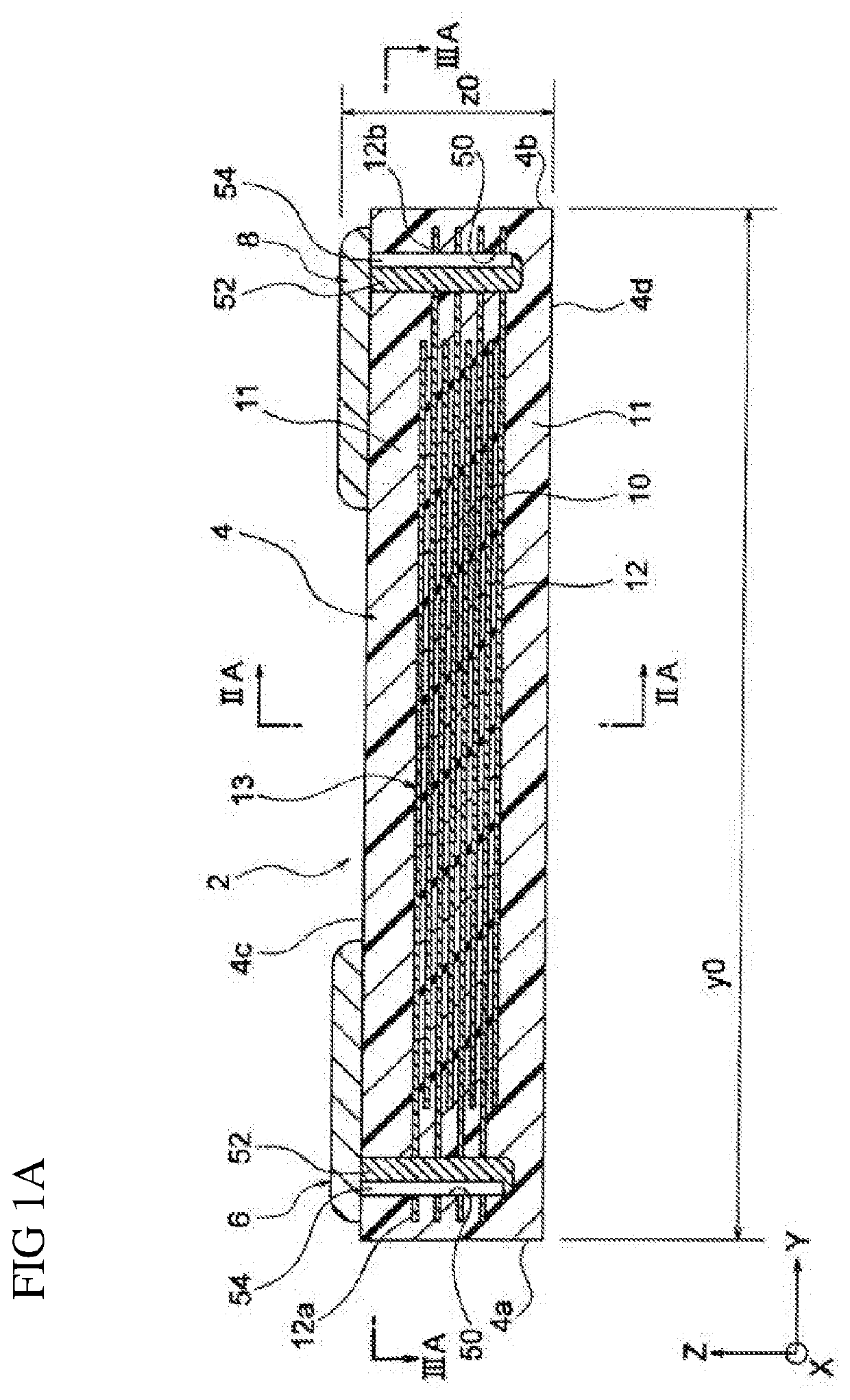
[0043]As an embodiment of a multilayer ceramic electronic component according to the present embodiment, a multilayer ceramic capacitor is described.
[0044]As shown in FIG. 1A, a multilayer ceramic capacitor 2 according to the present embodiment includes an element body 4, a first terminal electrode 6, and a second terminal electrode 8. The element body 4 includes inner dielectric layers (insulation layers) 10 and internal electrode layers 12 in substantially parallel to the plane including the X-axis and the Y-axis. The internal electrode layers 12 are alternately laminated along the Z-axis direction between the inner dielectric layers 10. Here, “substantially parallel” means that most part is parallel, but there may be a part that is not slightly parallel. The internal electrode layers 12 and the inner dielectric layers 10 may slightly be uneven or inclined.
[0045]An interior region 13 is a region where the inner dielectric layers 10 and the internal electrode layers 12 are alternat...
second embodiment
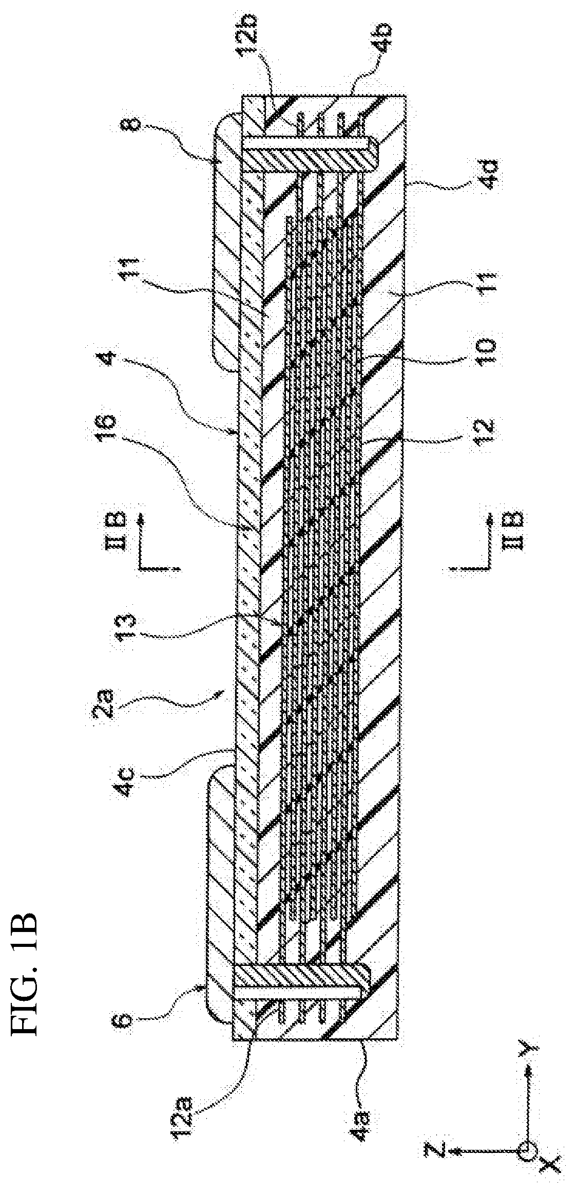
[0094]Except for the following matters, as shown in FIG. 1B and FIG. 2B, a multilayer ceramic capacitor 2a according to the present embodiment is similar to the multilayer ceramic capacitor 2 according to First Embodiment. In the multilayer ceramic capacitor 2a, the upper surface 4c (or the lower surface 4d) of the element body 4 includes an upper-surface reinforcement layer 16 made of a material that is stronger than the inner dielectric layers 10, and the outer surface of the upper-surface reinforcement layer 16 defines the upper surface 4c (or the lower surface 4d) of the element body 4.
[0095]After the element body 4 is formed similarly to First Embodiment, the upper-surface reinforcement layer 16 is formed on the upper surface 4c (or the lower surface 4d) of the element body 4 before the first and second terminal electrodes 6 and 8 are formed. The upper-surface reinforcement layer 16 is not limited and is glass, alumina based composite material, zirconia based composite material...
third embodiment
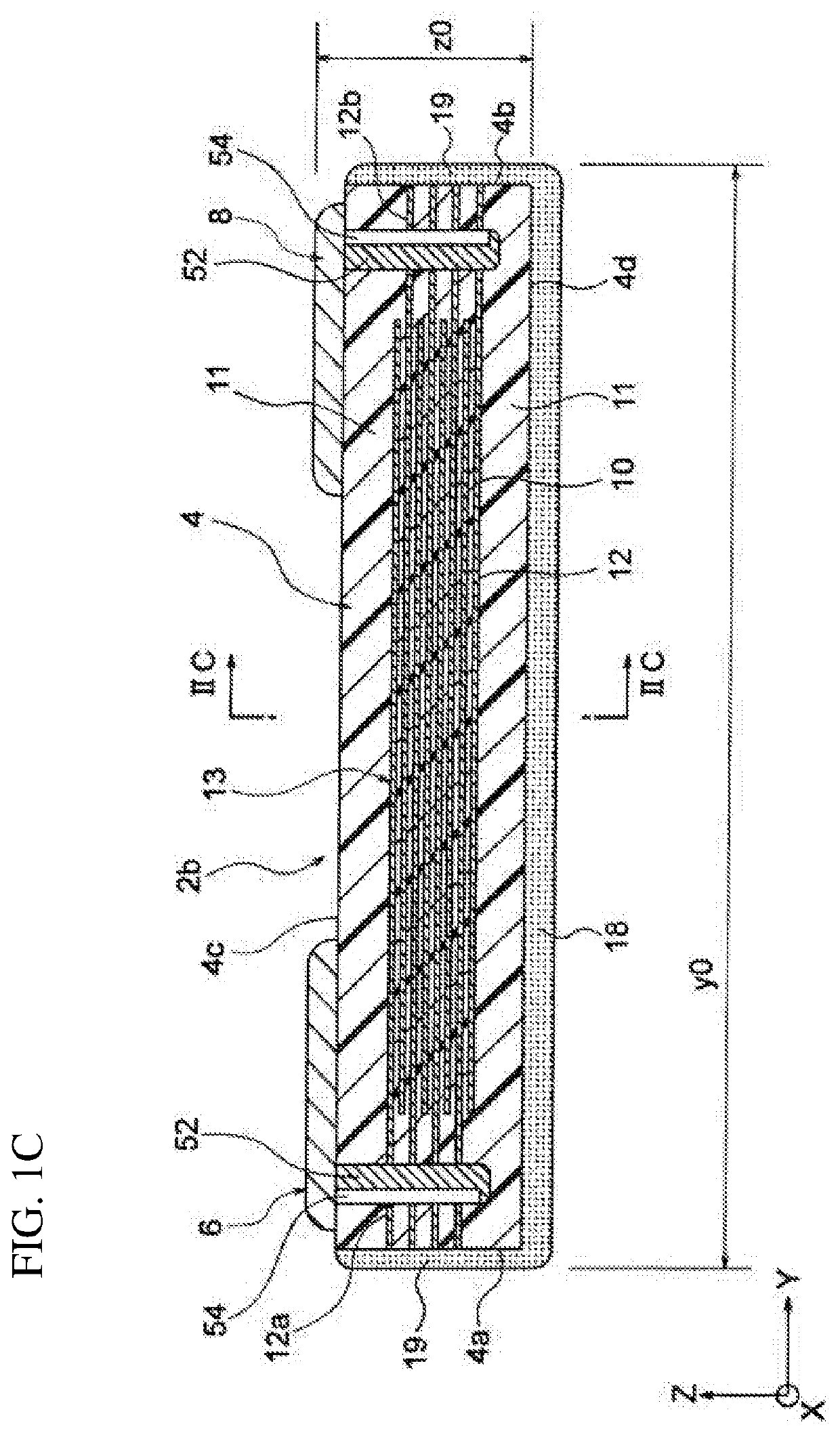
[0108]Except for the following matters, as shown in FIG. 1C and FIG. 2C, a multilayer ceramic capacitor 2b according to the present embodiment is similar to the multilayer ceramic capacitors 2 and 2a according to First Embodiment and Second Embodiment. In the capacitor 2b, a bottom reinforcement layer 18 is formed to cover the lower surface 4d of the element body 4, and lateral reinforcement layers 19 are formed continuously to the bottom reinforcement layer 18 so as to cover the first lateral surface 4a, the second lateral surface 4b, and the lateral surfaces 4e of the element body 4.
[0109]In the present embodiment, as shown in FIG. 2C, both ends of the internal electrode layers 12 in the X-axis direction are exposed from the lateral surfaces of the element body 4 in the X-axis direction, and the lateral reinforcement layers 19 are formed on the first lateral surface 4a, the second lateral surface 4b, and the lateral surfaces 4e of the element body 4 so as to cover the exposed port...
PUM
| Property | Measurement | Unit |
|---|---|---|
| Fraction | aaaaa | aaaaa |
| Percent by mass | aaaaa | aaaaa |
| Ratio | aaaaa | aaaaa |
Abstract
Description
Claims
Application Information