High frequency switch

a high-frequency switch and switch technology, applied in the field of high-frequency switches, can solve the problems of plurality of input/output terminals, deviation of insertion loss between the transfer paths connecting the common terminal, etc., and achieve the effect of easy realization, increased wiring length, and easy impedance matching

Active Publication Date: 2020-05-28
MURATA MFG CO LTD
View PDF4 Cites 0 Cited by
  • Summary
  • Abstract
  • Description
  • Claims
  • Application Information

AI Technical Summary

Benefits of technology

[0025]With that feature, it is easier to realize the configuration in which the differences in path lengths from the plurality of input / output terminals and the plurality of FETs to the common terminal are smaller. Furthermore, the length of the wiring connecting the common terminal to the common-terminal-dedicated external connection terminal can be increased and impedance matching can be more easily made.
[0026]According to the present disclosure, the deviation in insertion loss among the transfer paths connecting the common terminal and the plurality of input / output terminals individually can be reduced.

Problems solved by technology

However, when the high frequency switch is formed using a semiconductor, a deviation in insertion loss may occur among the transfer paths connecting the common terminal and the plurality of input / output terminals in some cases depending on the positional relations between the common terminal and the plurality of input / output terminals.

Method used


Image

  • High frequency switch
  • High frequency switch
  • High frequency switch

Examples


Embodiment Construction

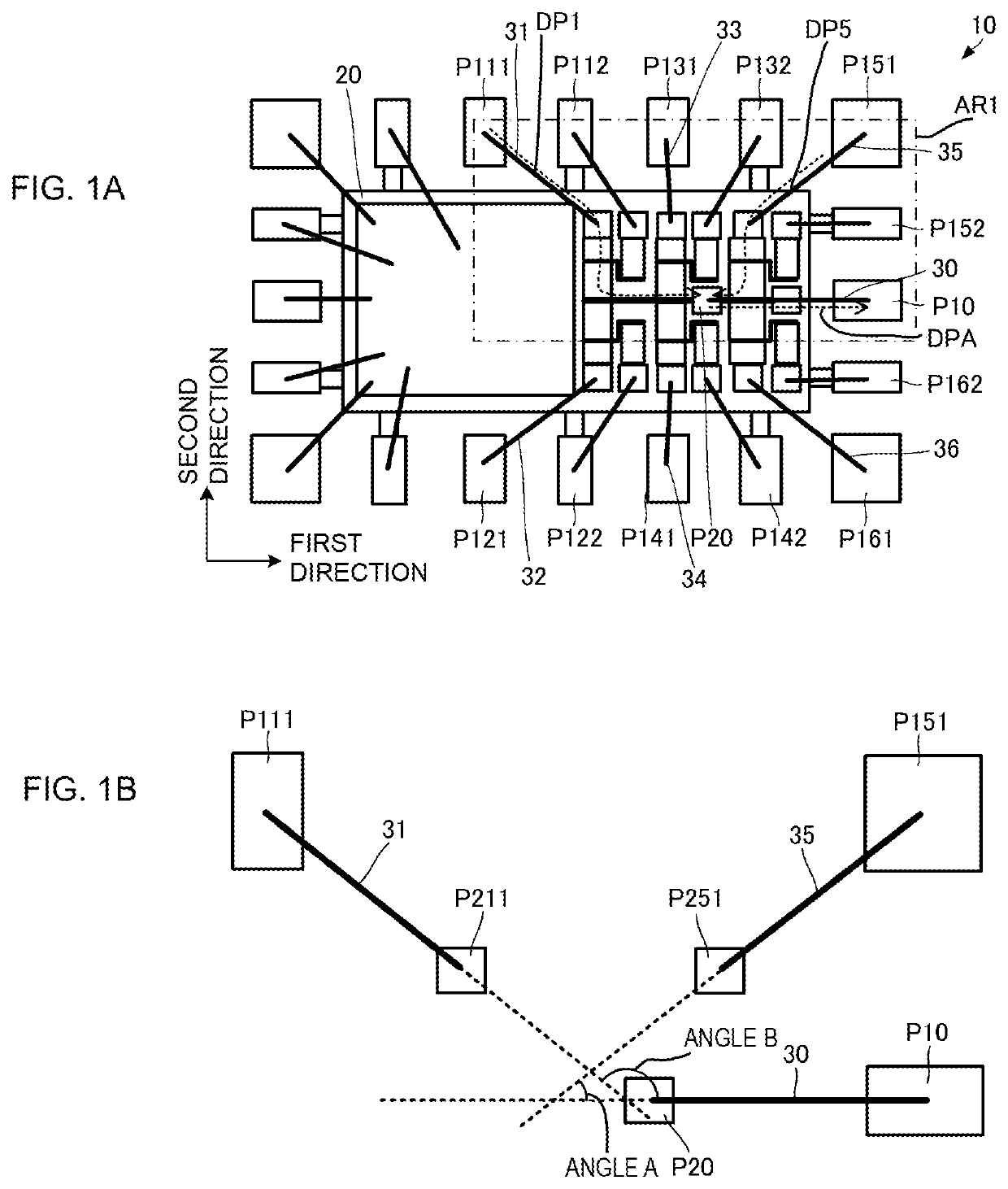
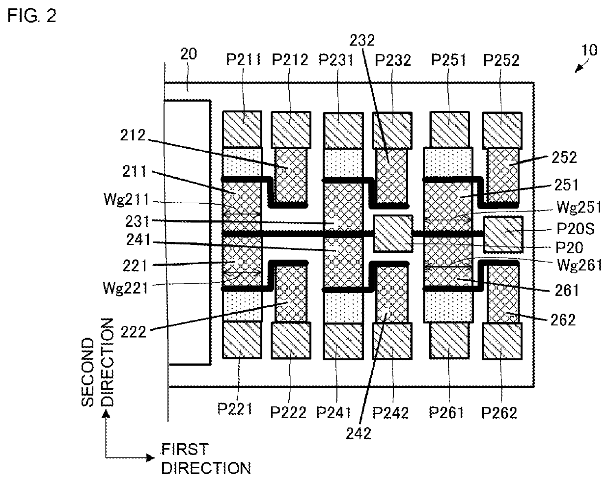
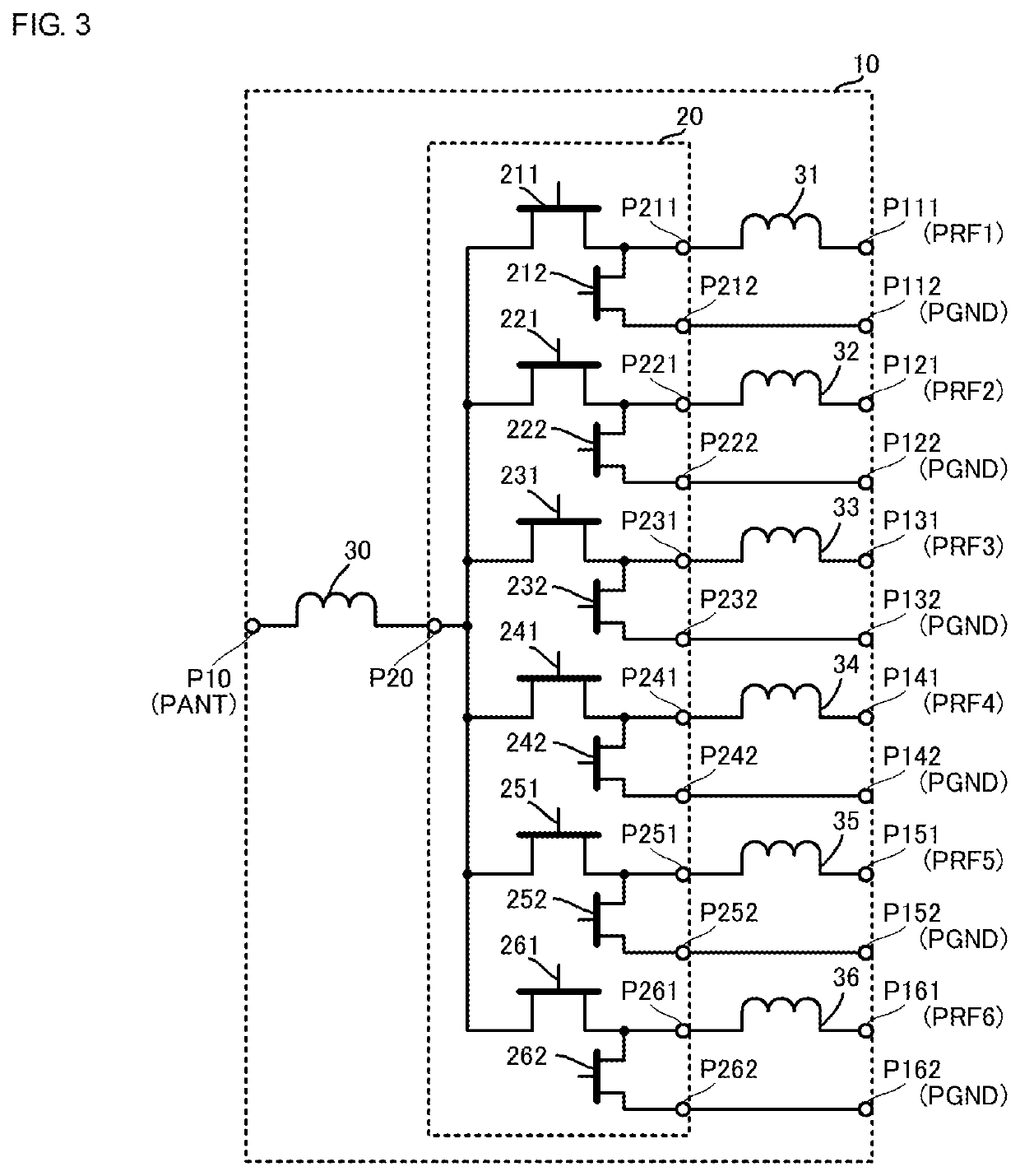
[0033]A high frequency switch according to a first embodiment of the present disclosure will be described below with reference to the drawings. FIG. 1A is a plan view illustrating a layout of individual terminals and power propagation directions in a high frequency switch 10 according to the first embodiment of the present disclosure. FIG. 1B is a partial enlarged view illustrating, in an enlarged scale, a portion corresponding to an area AR1 in FIG. 1A. For easier understanding of the features illustrated in FIG. 1B, only necessary components are illustrated, and other components are omitted in FIG. 1B. FIG. 2 is a plan view illustrating, in an enlarged scale, a portion of a semiconductor element 20 in the high frequency switch 10 according to the first embodiment of the present disclosure. FIG. 3 is a circuit diagram of the high frequency switch 10 according to the first embodiment of the present disclosure.

[0034](Circuit Configuration of High Frequency Switch)

[0035]The high frequ...


PUM


Abstract

A length of a zone in which a power propagation direction from an input/output terminal (P251) toward a common terminal (P20) and a power propagation direction from the common terminal (P20) toward an external connection terminal (P10) are opposite to each other is longer than a length of a zone in which a power propagation direction from an input/output terminal (P211) toward the common terminal (P20) and a power propagation direction from the common terminal (P20) toward the external connection terminal (P10) are opposite to each other. A FET (251) and a FET (211) have structures that power transferred between a drain and a source of the FET (251) in accordance with predetermined input power is greater than power transferred between a drain and a source of the FET (211).

Description

[0001]This is a continuation of International Application No. PCT / JP2018 / 028071 filed on Jul. 26, 2018 which claims priority from Japanese Patent Application No. 2017-148755 filed on Aug. 1, 2017. The contents of these applications are incorporated herein by reference in their entireties.BACKGROUND OF THE DISCLOSUREField of the Disclosure[0002]The present disclosure relates to a high frequency switch selectively connecting a plurality of input / output terminals to a common terminal.Description of the Related Art[0003]Up to now, a high frequency switch is often utilized in a high frequency module. For example, the high frequency switch is connected between an antenna common to multiple types of communication signals and a transmitting / receiving circuit arranged for each of the multiple types of communication signals. The high frequency switch includes a common terminal and a plurality of input / output terminals. The common terminal is connected to the antenna, and the plurality of inpu...

Claims


Application Information

Patent Timeline
Patent Type & Authority Applications(United States)
IPC IPC(8): H03K17/693
CPCH04B1/48H03K17/693H03K17/162H03K17/6871H01L21/822H01L27/04H01P1/15
Inventor SEKI, KENTA
Owner MURATA MFG CO LTD
Why Eureka
Try Eureka