Method of forming a structure including silicon nitride on titanium nitride and structure formed using the method

a technology of titanium nitride and silicon nitride, which is applied in the direction of superimposed coating process, chemical vapor deposition coating, coating, etc., can solve the problems of oxidation of titanium nitride material, relatively high procedure cost, and general less desirable metal film of mos device, etc., and achieve the effect of mitigating the oxidation of titanium nitride film

Pending Publication Date: 2020-06-11
ASM IP HLDG BV
View PDF13 Cites 204 Cited by
  • Summary
  • Abstract
  • Description
  • Claims
  • Application Information

AI Technical Summary

Benefits of technology

[0005]Various embodiments of the present disclosure relate to methods of mitigating undesired oxidation of titanium nitride films. While the ways in which various embodiments of the present disclosure address drawbacks of prior methods are discussed in more detail below, in general, various embodiments of the disclosure provide in situ methods of capping the titanium nitride layer with material less prone to oxidation and / or that mitigates oxidation of the titanium nitride film.
[0006]In accordance with exemplary embodiments of the disclosure, a method of forming a structure includes providing a substrate in a reaction chamber, forming a layer comprising titanium nitride overlying the substrate in the reaction chamber, and forming a layer comprising silicon nitride overlying the layer comprising titanium nitride in the reaction chamber. The step of forming the layer comprising titanium nitride and the step of forming the layer comprising silicon nitride are performed within the same reaction chamber—e.g., without exposing the substrate to another intervening environment (e.g., a substrate transfer region of a processing tool or the like) or exposing the substrate to an intervening vacuum break. The step of forming the layer comprising silicon nitride can include a cyclic deposition step, such as atomic layer deposition. In accordance with various aspects of these embodiments, the step of forming the layer comprising silicon nitride can be self-limiting, i.e., the growth of the silicon nitride layer can substantially stop after the silicon nitride layer reaches a certain thickness—e.g., about 2 Angstroms in some cases. In accordance with further aspects, a thickness of the silicon nitride layer is greater than 0 and less than 5 Angstroms. Because the titanium nitride and the silicon nitride layers are deposited in the same reaction chamber, the deposition conditions (e.g., pressure, temperature) can be about the same (e.g., within ten, five, two, one, or one half of a percent). The titanium nitride layer can be formed over high dielectric constant material, such as hafnium oxide and / or work function layers, such as titanium carbide, titanium aluminum carbide, or the like. In accordance with yet additional aspects of these embodiments, the step of forming the layer comprising titanium nitride and the step of forming the layer comprising silicon nitride can be repeated, individually and / or collectively, a number of times to form a laminate structure formed from deposited layers of titanium nitride and silicon nitride.
[0007]In accordance with additional embodiments of the disclosure, a structure including a titanium nitride layer and a silicon nitride layer is formed according to a method disclosed herein. Exemplary structures can include, for example, a channel region (e.g., a silicon germanium channel region), a high dielectric constant layer (e.g., comprising a high dielectric constant material as described herein) overlying the channel region, a layer comprising titanium nitride layer overlying the high dielectric constant layer, and a silicon nitride layer formed overlying (e.g., in contact with) the titanium nitride layer.

Problems solved by technology

The titanium oxynitride films exhibit a higher resistivity than titanium nitride films, and thus are generally less desirable for metal films of a MOS device.
However, such procedures are relatively expensive and require modifications to processing tools to provide adequate sealing.
Further, such techniques can still allow undesirable amounts of oxidation of the titanium nitride material prior to subsequent processing.

Method used


Image

  • Method of forming a structure including silicon nitride on titanium nitride and structure formed using the method
  • Method of forming a structure including silicon nitride on titanium nitride and structure formed using the method
  • Method of forming a structure including silicon nitride on titanium nitride and structure formed using the method

Examples


Embodiment Construction

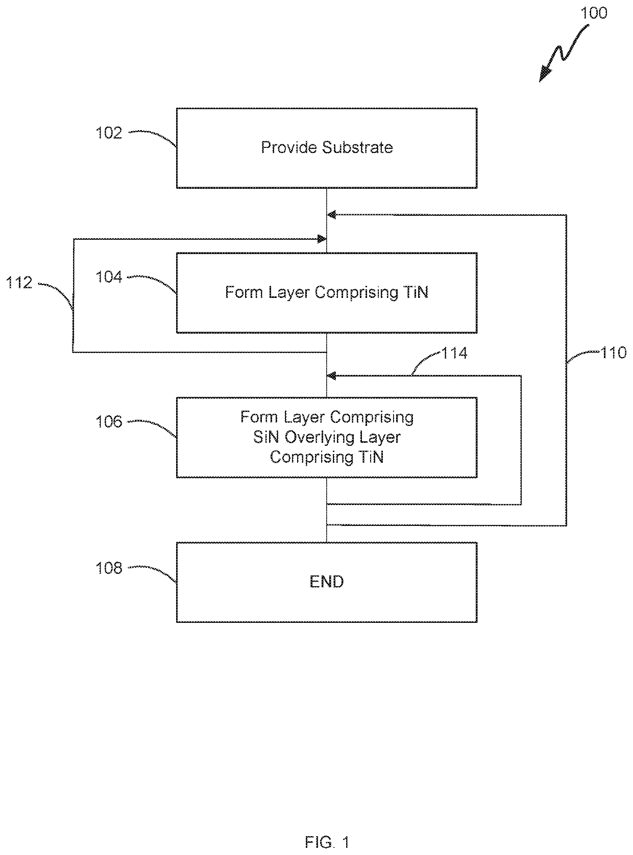
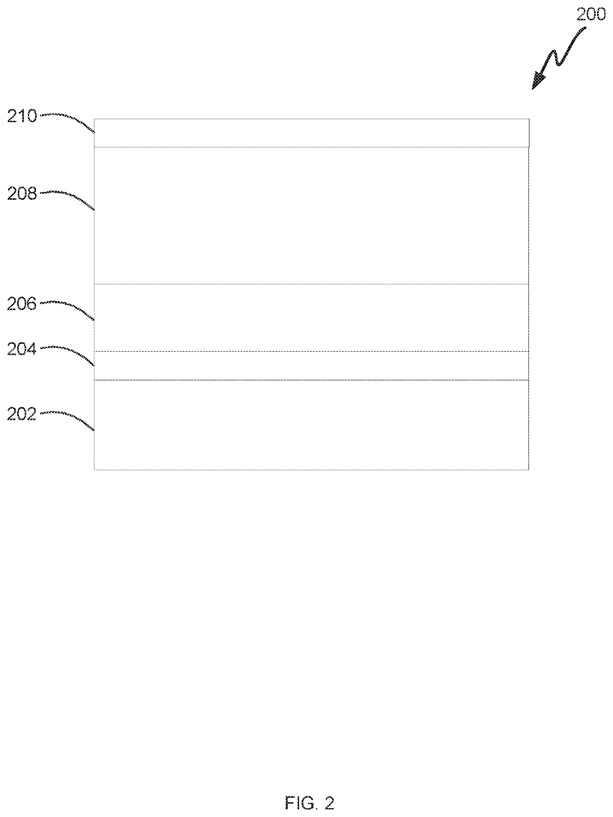
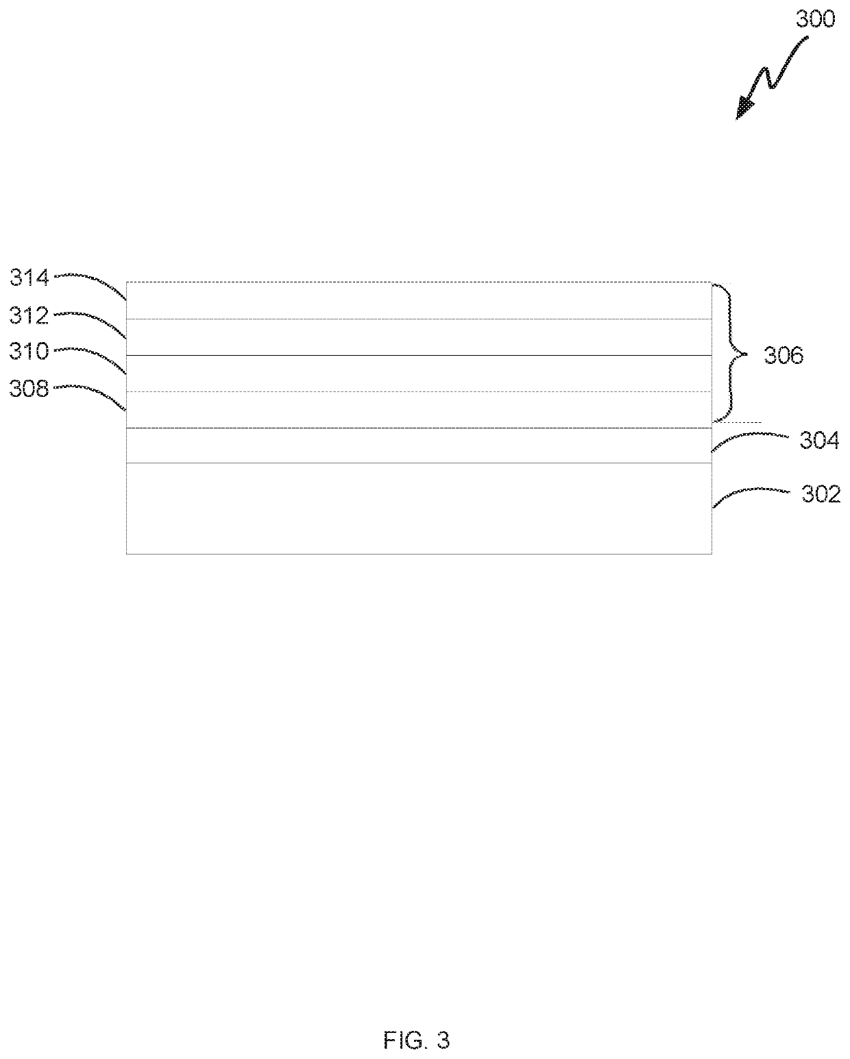
[0013]The description of exemplary embodiments provided below is merely exemplary and is intended for purposes of illustration only; the following description is not intended to limit the scope of the disclosure or the claims. Moreover, recitation of multiple embodiments having stated features is not intended to exclude other embodiments having additional features or other embodiments incorporating different combinations of the stated features. Further, the illustrations presented herein are not meant to be actual views of any particular material, structure, or device, but are merely idealized representations that are used to describe embodiments of the disclosure.

[0014]The present disclosure generally relates to methods of forming structures and to structures formed using the methods. As set forth in more detail below, the methods and structures described herein can be used to form, for example, MOS devices having high-mobility channel material (e.g., silicon germanium) with relati...


PUM

PropertyMeasurementUnit
thicknessaaaaaaaaaa
temperatureaaaaaaaaaa
thicknessaaaaaaaaaa

Abstract

A method of forming a structure including a silicon nitride overlying a titanium nitride layer is disclosed. The method includes forming the titanium nitride layer and the silicon nitride layer in the same reaction chamber—e.g., without a vacuum break—to mitigate oxidation of the titanium nitride layer that might otherwise occur.

Description

FIELD OF THE DISCLOSURE[0001]The present disclosure generally relates to thin-film deposition methods and structures. More particularly, the disclosure relates to methods of forming silicon nitride capping layers on titanium nitride films and to structures including such layers and films.BACKGROUND OF THE DISCLOSURE[0002]Titanium nitride films can be used as a metal or conducting layer in a variety of applications. For example, titanium nitride films can be used as a metal layer in a metal oxide semiconductor (MOS) device or a structure forming part of such device. Use of the titanium nitride film or layer in such structures may be desirable, particularly in cases in which a channel region of the MOS device includes silicon germanium, because the titanium nitride layer exhibits oxygen-scavenging properties, which can be desirable to reduce interface trapped charge density (Dit) across a band gap of such structures and / or reduce equivalent oxide thickness (EOT). Titanium nitride laye...

Claims


Application Information

Patent Timeline
Patent Type & Authority Applications(United States)
IPC IPC(8): C23C16/34H01L21/02C23C16/455
CPCH01L29/518H01L29/513H01L21/02186C23C16/45525C23C16/345H01L21/0217H01L21/0228H01L21/28255H01L29/4966H01L29/78H01L21/02274H01L29/517H01L21/28088C23C28/04C23C28/042H01L21/02172H01L21/28194H01L21/324
Inventor LONGRIE, DELPHINETANG, FU
Owner ASM IP HLDG BV
Why Eureka
Try Eureka