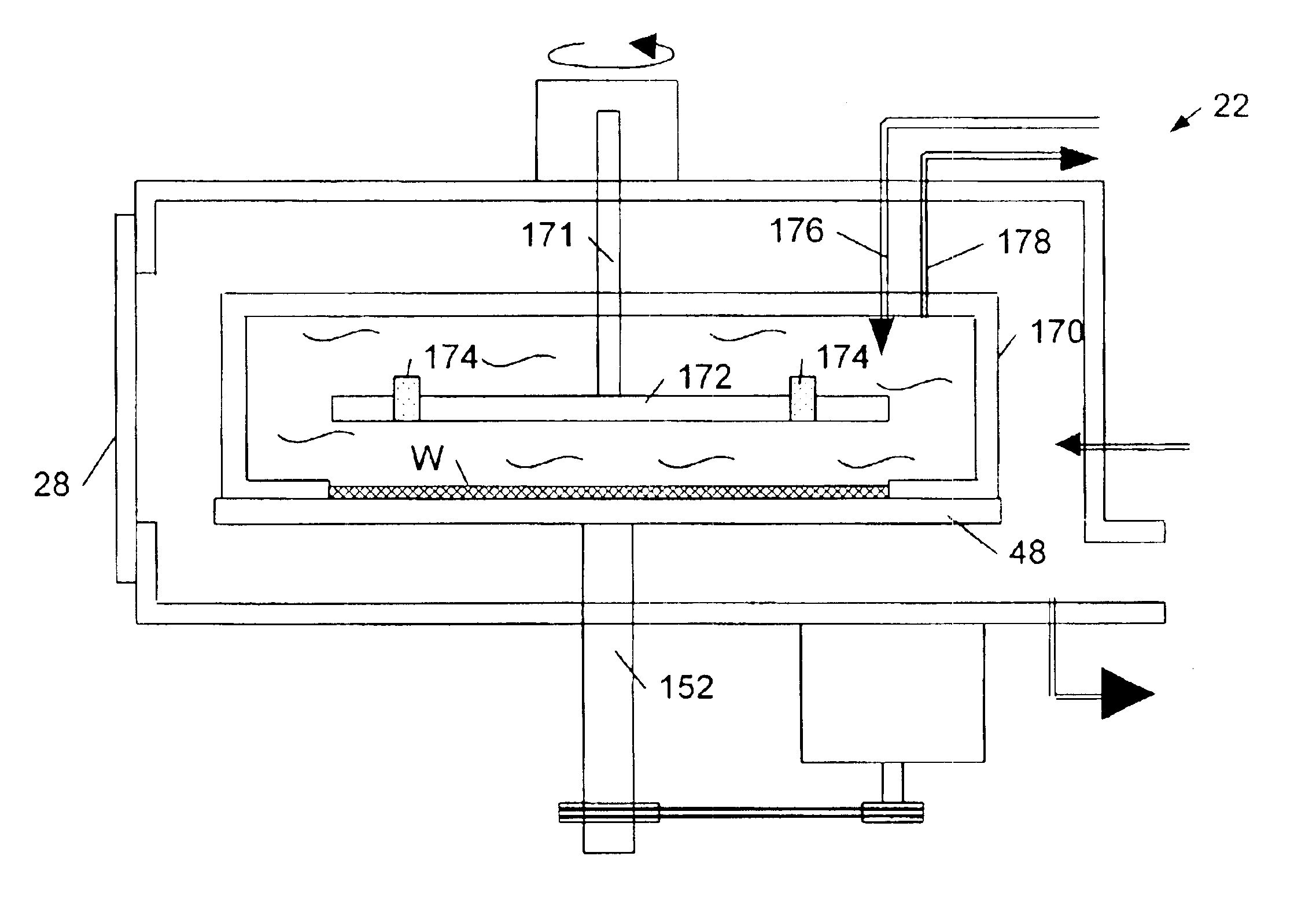
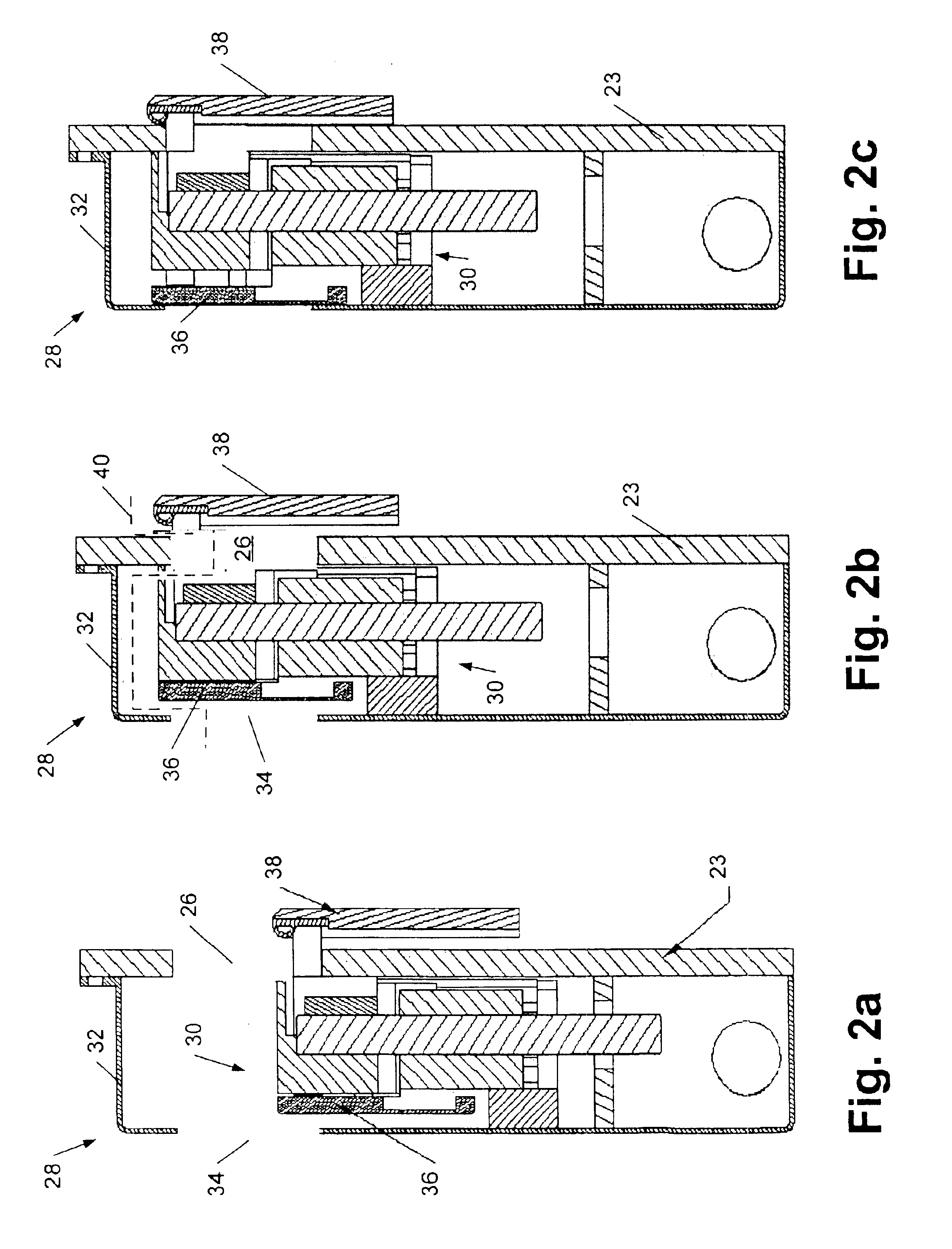
In either case, the process chamber may further include a gate latch configured to align barriers of the gate latch with the wall opening and the gate casing opening. In some embodiments, the gate latch is configured to move within the space between the wall
and gate casing. In this manner, the gate latch may be configured to move the barriers such that the barriers are not in alignment with the wall opening
and gate casing opening as well. In some cases, the portion of the gate latch comprising the barriers may be configured to move such that the two openings are either sealed or provide an air passage to the process chamber when the barriers are respectively aligned with the two openings. In this manner, the barriers may prevent fluids within the process chamber from flowing through the wall opening
and gate casing opening whenever the barriers are respectively aligned with the two openings. In some embodiments, the process chamber may be adapted to draw air through the air passage and into the process chamber.
In general, the
system described herein may be adapted to provide any process fluid for processing a microelectronic topography to a process chamber, including liquids, gases, and / or plasmas. In some embodiments, it may be particularly advantageous to perform a process using a
single phase. For example, employing a single
liquid phase environment may offer a manner with which to control the pressure within the process chamber. In general, increasing the pressure of a solution may advantageously increase the
boiling point of the solution. In embodiments of electroless deposition, an increase in the
boiling point of the deposition solution may increase the temperature at which the solution decomposes and may further allow the rate of deposition to be increased. As such, a method for electrolessly depositing a layer upon a microelectronic topography exclusively using a
liquid phase is contemplated herein. In general, the method may include loading the
wafer into an electroless
deposition chamber, sealing the electroless
deposition chamber to form an enclosed area about the microelectronic topography, and filling the enclosed area with a deposition solution. In some cases, filling the chamber may include pressurizing the enclosed area to a pressure between approximately 5 psi and approximately 100 psi, increasing the
boiling point of the deposition solution. In some embodiments, the method heating the deposition solution to a temperature less than approximately 25% below the boiling point of the deposition solution to increase a
reaction rate of the deposition solution with the microelectronic topography.
In some cases, pressurizing the chamber may be advantageous for minimizing the generation and accumulation of bubbles upon a surface of a
wafer during an electroless
deposition process. In addition or alternatively, positioning a wafer face-up within a processing chamber may reduce generation and accumulation of bubbles upon a wafer. In yet other embodiments, agitating a solution used for an electroless
deposition process may further or alternatively minimize the generation and accumulation of bubbles upon a wafer surface. As such, a method may minimizing the accumulation of bubbles upon a wafer during an electroless
deposition process is provided herein. In general, the method may include loading the wafer into an electroless
deposition chamber, sealing the electroless deposition chamber to form an enclosed area about the wafer, and supplying a deposition solution to the enclosed area. In addition, the method may include agitating the deposition solution to create an amount of motion sufficient to form a layer having substantially uniform thickness. In some cases, the method may further include pressurizing the enclosed area to a predetermined value, such as between approximately 5 psi and approximately 100 psi. In this manner, the steps of agitating and pressurizing may collectively reduce the amount of bubbles formed upon the wafer during the electroless deposition process. In addition or alternatively, the step of loading the wafer may include positioning the wafer face-up within the electroless deposition chamber such that the generation of bubbles may be further reduced.
Another microelectronic topography which may be formed using the methods described herein may include a metal feature having a single layer comprises at least four elements lining a lower surface and sidewalls of the metal feature. In some embodiments, the single
barrier layer may include at least four elements selected from a group consisting of
boron,
chromium,
cobalt,
molybdenum,
nickel,
phosphorus,
rhenium, and
tungsten. In addition, the concentration of elements within the single barrier layer may include three elements each comprising between approximately 0.1% and approximately 20% of a
molar concentration of the barrier layer and a fourth element comprising the balance of the
molar concentration. In some embodiments, the fourth element may include
cobalt or
nickel. In some embodiments, the single barrier layer may be configured to substantially prevent oxidation. In addition or alternatively, the single barrier layer may be configured to substantially prevent
diffusion of a bulk metal layer formed upon the single barrier layer to other
layers within the microelectronic topography. In some embodiments, the metal feature may further include a second single barrier layer comprising at least four elements arranged upon and in contact with the bulk metal layer.
There may be several advantages to using the
system and methods described herein. For example, a system is provided which is adapted to conduct one or more process steps within a chamber without removing the wafer arranged within the chamber. In this manner, the deposition of foreign particles and oxidation of the topography may be minimized. In addition, a process chamber is provided which prevents process solutions from mixing upon being dispensed from the process chamber. Consequently, one or more of the process fluids used in the process chamber may be recycled, reducing material and
waste disposal costs associated with the process. Moreover, a substrate holder is provided which is adapted to secure a wafer within a chamber such that a wafer is not damaged during processing. In addition, a gate adapted to provide an air passage to the process chamber during processing is provided. In this manner,
ambient air exterior to the process chamber may be supplied to the process chamber for a
drying process, for example. Furthermore, a method and a system for reducing the generation and accumulation of bubbles upon a wafer surface during processing is provided. As a result, a substantially uniform layer may be deposited. In some cases, the method and system described herein may increase the boiling point of an electroless deposition solution used within a process chamber. Such an increase in the boiling point may, in some embodiments, may be used to increase the
deposition rate of the layer, increasing production
throughput of the system.
Additional benefits may also be realized by the method of hydrating the barrier layer prior to an electroless deposition process. In particular, such a process may advantageously allow the barrier layer to be readily available for the deposition of a catalytic seed layer while preventing the accumulation of particulate matter upon the barrier layer. Consequently, a more uniform bulk metal layer may be deposited thereon. In embodiments in which the barrier is formed to include at least four elements, the barrier layer may be autocatalytic and, therefore, may not need the extraneous process steps of activating the barrier layer. Furthermore, the method which deposits a hydrophobic layer upon
dielectric portion of the topography prior to the deposition of a cap layer may advantageously prevent the deposition of a the layer upon dielectric portions of a topography, potentially preventing the formation of a short within the device.

