Photo-detecting apparatus with multi-reset mechanism cross-reference to related applications

a multi-reset mechanism and photo-detecting technology, applied in the field of photo-detecting apparatuses, can solve the problems of reducing the signal to noise ratio, increasing power consumption, and affecting the and achieves the effects of low dark current, small chip size, and improved accuracy of 3d image depth information

Active Publication Date: 2020-06-18
ARTILUX INC
View PDF0 Cites 7 Cited by
  • Summary
  • Abstract
  • Description
  • Claims
  • Application Information

AI Technical Summary

Benefits of technology

[0010]Among other advantages and benefits of the embodiments disclosed herein, the embodiments provide a photo-detecting apparatus capable of absorbing a least a near-infrared (NIR) light or a short-wave infrared (SWIR) light efficiently. In some embodiments, the photo-detecting apparatus may have smaller chip size, low dark current and / or higher accuracy of the 3D image depth information, and low leakage current and / or lower consumption of the 3D image sensor power.

Problems solved by technology

However, when photodetectors are applied to these applications in a single or array configuration, the leakage current and dark current may degrade performances such as increasing the power consumption and reducing the signal to noise ratio.

Method used


Image

  • Photo-detecting apparatus with multi-reset mechanism cross-reference to related applications
  • Photo-detecting apparatus with multi-reset mechanism cross-reference to related applications
  • Photo-detecting apparatus with multi-reset mechanism cross-reference to related applications

Examples


Embodiment Construction

General Structure of One-Tap Configuration

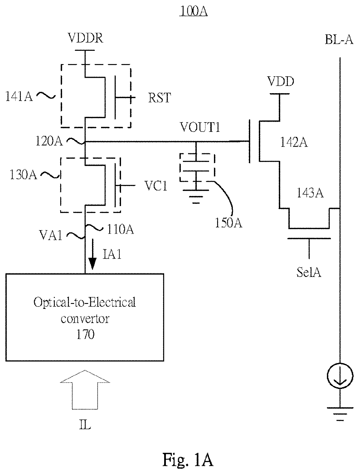
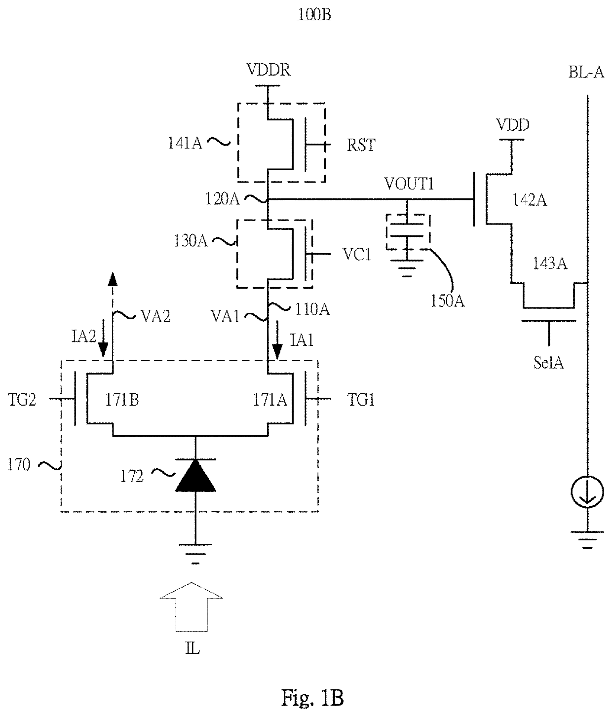
[0018]FIG. 1A illustrates a photo-detecting apparatus 100A with one-tap configuration, according to some embodiments. The photo-detecting apparatus 100A includes an optical-to-electric converter 170, a cascode transistor 130A, a reset transistor 141A, a source-follower transistor 142A, a row-select transistor 143A, a capacitor 150A and a bit-line BL-A.

[0019]The optical-to-electric converter 170 is configured to convert an incident light IL to an electrical signal IA1 at an output terminal 110A, where the electrical signal IA1 is a photo-current. There are many implementations for the optical-to-electric converter 170, the details will be described hereinafter. The cascode transistor 130A is coupled between the optical-to-electric converter 170 and the reset transistor 141A. Specifically, one channel terminal (e.g., source terminal) of the cascode transistor 130A is coupled to the output terminal 110A of the optical-to-electric converter 170 ...


PUM


Abstract

A photo-detecting apparatus includes an optical-to-electric converter, having a first output terminal, configured to convert an incident light to an electrical signal; a cascode transistor, having a control terminal, a first channel terminal and a second channel terminal, wherein the second channel terminal of the cascode transistor is coupled to the first output terminal of the optical-to-electric converter; and a reset transistor, having a control terminal, a first channel terminal and a second channel terminal, wherein the first channel terminal of the reset transistor is coupled to a supply voltage and the second channel terminal of the reset transistor is coupled to the first channel terminal of the cascode transistor.

Description

CROSS REFERENCE TO RELATED APPLICATIONS[0001]This patent application claims the benefit of U.S. Provisional Patent Application No. 62 / 778,291, filed Dec. 12, 2018, U.S. Provisional Patent Application No. 62 / 807,250, filed Feb. 19, 2019, U.S. Provisional Patent Application No. 62 / 875,941, filed Jul. 18, 2019, which are incorporated by reference herein.BACKGROUND OF THE INVENTION1. Field of the Invention[0002]The present invention relates to a photo-detecting apparatus, and more particularly, to a photo-detecting apparatus with a multi-reset mechanism.2. Description of the Prior Art[0003]Photo-detecting apparatus may be used to detect incident light and convert the incident light to electrical signal that may be further processed by another circuitry. Photodetectors may be used in consumer electronics products, image sensors, data communications, time-of-flight (ToF), light detection and ranging (LiDAR), medical devices, and many other suitable applications. However, when photodetecto...

Claims


Application Information

Patent Timeline
Patent Type & Authority Applications(United States)
IPC IPC(8): G02B6/35H04N5/3745G02B6/42
CPCG02B6/3582H04N5/3745G02B6/4292G05F3/08H01L27/1446H01L27/14612G01S17/894G01S17/36G01S7/4913H04N25/77
Inventor NA, YUN-CHUNGLIANG, CHE-FUCHEN, CHIEN-LUNGLYU, YUAN-FULU, YEN-CHENG
Owner ARTILUX INC
Why Eureka
Try Eureka