
Ldmos device and manufacturing method thereof

a technology of ldmos and manufacturing method, which is applied in the direction of semiconductor devices, basic electric elements, electrical apparatus, etc., to achieve the effect of improving the breakdown voltage of the devi

Active Publication Date: 2020-08-27
SEMICONDUCTOR MANUFACTURING INTERNATIONAL (BEIJING) CORP +1
View PDF0 Cites 0 Cited by
  • Summary
  • Abstract
  • Description
  • Claims
  • Application Information

AI Technical Summary

Benefits of technology

The technical solution of the present disclosure provides a method for manufacturing an LDMOS device with an increased device breakdown voltage without increasing the risk of breakdown in certain areas. This is achieved by using an isolation structure between the drain region and the gate structure, which allows for the placement of a groove electrode and also increases the thickness of the isolation layer between the substrate and the electrodes. This arrangement does not change any other parts of the semiconductor structure, such as the functional region layout or ion implantation concentration, which helps to maintain the device's efficiency while improving its breakdown voltage.

Problems solved by technology

Thus, how to improve BVDss, but not increase Rdson becomes a problem urgently needing to be solved.

Method used


Image

  • Ldmos device and manufacturing method thereof
  • Ldmos device and manufacturing method thereof
  • Ldmos device and manufacturing method thereof

Examples


Embodiment Construction

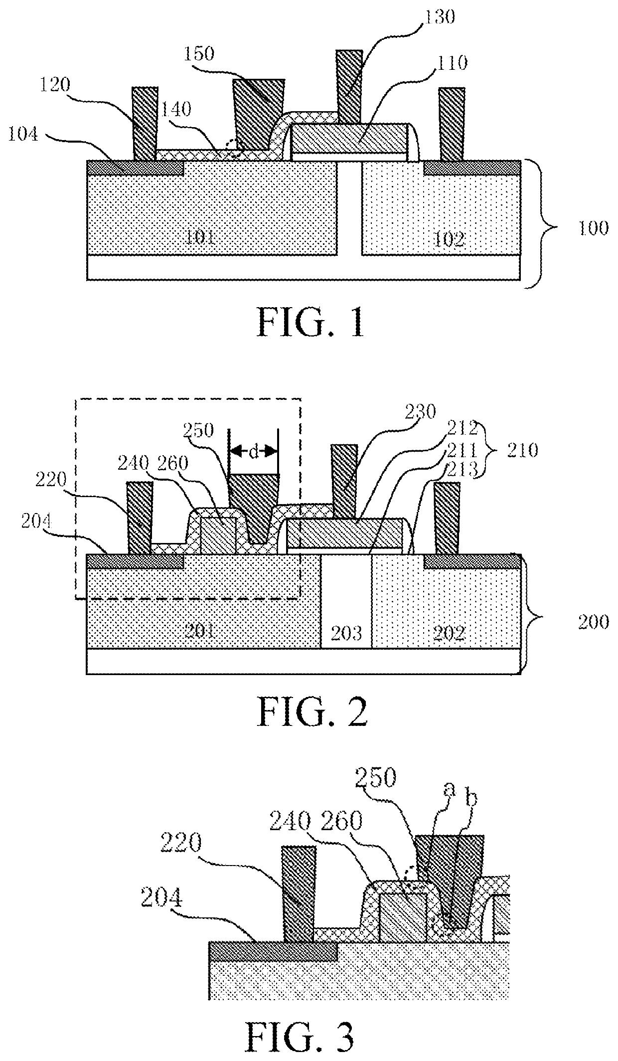
[0019]FIG. 1 illustrates a structural schematic view of an LDMOS device. The LDMOS device includes: a substrate 100, a drift region 101 and a well region 102 isolated from each other formed in the substrate 100; a gate structure 110, located at a junction of the drift region 101 and the well region 102 and covering part of the drift region 101 and the well region 102; a drain region 104, located in the drift region 101 on one side of the gate structure 110, the drain region 104 isolated from the gate structure 110; a drain electrode 120, located on the drain region 104 and electrically connected with the drain region 104; a gate electrode 130, located on the gate structure 110 and electrically connected with the gate structure 110; a salicide block (SAB) layer 140, located on the drift region 101 and the gate structure 110 between the drain electrode 120 and the gate electrode 130; and a groove electrode 150 located on the SAB layer 140 on one side of the gate structure 110.

[0020]Th...


PUM


Abstract

The present disclosure provides an LDMOS device and a manufacturing method thereof. The LDMOS device includes: a substrate, a drift region formed in the substrate; a gate structure, located on the substrate on one side of the drift region, and covering part of the drift region; a drain region, located in the drift region on one side of the gate structure, an isolation structure located on the substrate, the isolation structure located between the drain region and the gate structure; a gate electrode, located on the gate structure and electrically connected with the gate structure; a drain electrode, located on the drain region and electrically connected with the drain region; a block layer, covering the drift region and the isolation structure between the gate electrode and the drain electrode in a shape-preserving manner; and a groove electrode located on the block layer, the groove electrode located between the isolation structure and the gate structure, and at least covering part of the top of the isolation structure. The LDMOS device improves a device breakdown voltage, and cannot increase Rdson.

Description

RELATED APPLICATIONS[0001]The present application claims priority to Chinese Patent Appln. No. 201910141854.4, filed Feb. 26, 2019, the entire disclosure of which is hereby incorporated by reference.BACKGROUNDTechnical Field[0002]Embodiments and implementations of the present disclosure relates to the field of semiconductor manufacturing, and particularly relates to an LDMOS device and a manufacturing method thereof.Related Art[0003]An LDMOS (Laterally Diffused Metal Oxide Semiconductor) transistor is widely applied into a power integrated circuit because it is easier to be compatible with a logic process of CMOS (Complementary Metal Oxide Semiconductors). In the power integrated circuit, a BVDss-Rdson characteristic of a device has important significance for designing efficient power application circuits.[0004]Generally, Rdson and BVDss of an LDMOS are two mutually restricted performances. If Rdson is decreased, BVDss is very likely to be lowered, and vice versa. Thus, how to impro...

Claims


Application Information

Patent Timeline
IPC IPC(8): H01L29/78H01L29/66H01L29/40
CPCH01L29/66681H01L29/7816H01L29/402H01L29/0684H01L29/0642H01L29/7835H01L29/66659H01L29/665
Inventor CHEN, DEYANLI, MAOKOH, LEONG TEEJUNG, DAE-SUB
Owner SEMICONDUCTOR MANUFACTURING INTERNATIONAL (BEIJING) CORP
Learn More