
Electronic device

a technology of electronic devices and cases, applied in the direction of fixed capacitor details, stacked capacitors, fixed capacitors, etc., can solve the problems that electronic devices are not always convenient for users, and achieve the effect of easy connection and simplified case configuration

Active Publication Date: 2020-09-17
TDK CORPARATION
View PDF4 Cites 3 Cited by
  • Summary
  • Abstract
  • Description
  • Claims
  • Application Information

AI Technical Summary

Benefits of technology

The patent describes a technology that allows multiple electronic devices to be joined together by connecting them using cases. This creates a single unit that is easy for users to handle and can be configured in different ways for different uses. The connections between the cases are secure and can be increased or decreased easily. Additionally, the technology allows for easy interconnection of chip components within the cases. This simplifies the configuration of the cases and allows for easy connection of the chip components in series or parallel.

Problems solved by technology

Accordingly, the electronic devices are not always convenient for users in a case where it is desired to handle a plurality of the electronic devices as a single unit.

Method used


Image

  • Electronic device
  • Electronic device
  • Electronic device

Examples


first embodiment

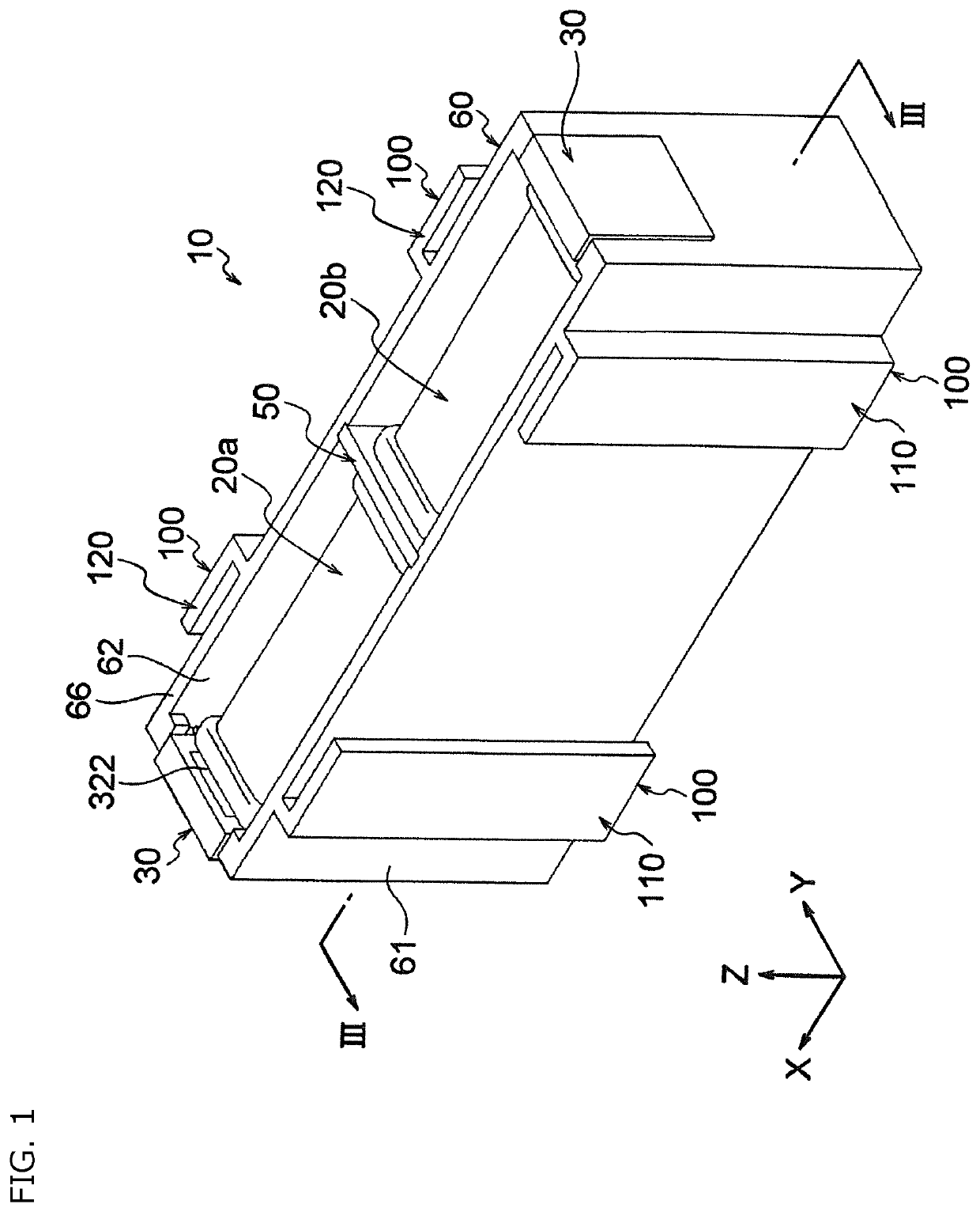
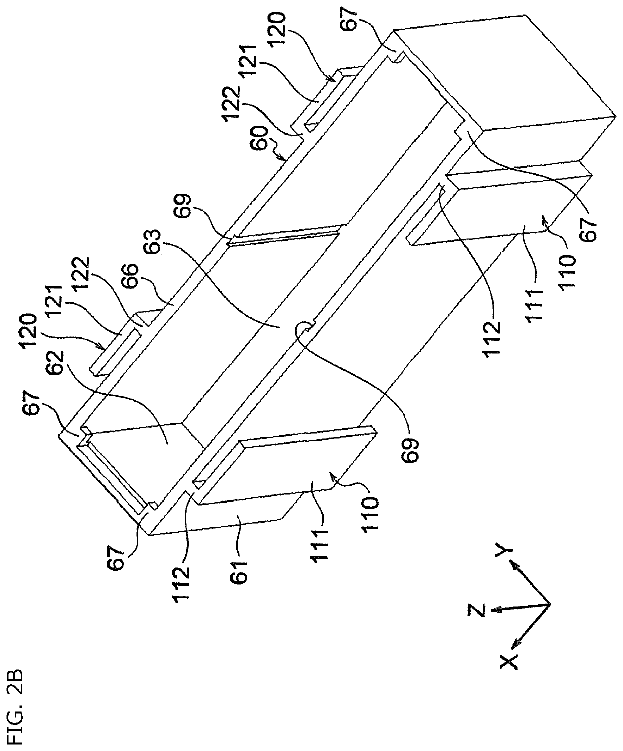
[0057]As illustrated in FIG. 1, an electronic device 10 according to a first embodiment of the invention has two capacitor chips (chip components) 20a and 20b, a pair of individual metal terminals 30 and 30, an intermediate connector 50, and an insulation case 60.

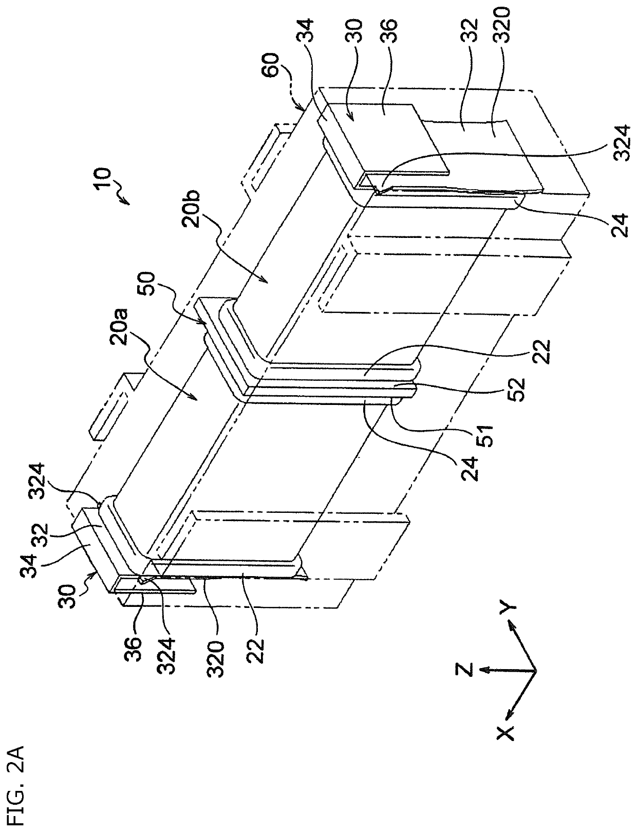
[0058]As illustrated in FIG. 2A, each of the capacitor chips 20a and 20b has a substantially rectangular parallelepiped shape and the capacitor chips 20a and 20b have substantially the same shape and size. As illustrated in FIG. 3, each of the capacitor chips 20a and 20b has an element main body in which inner electrode layers 26 and dielectric layers 28 are stacked along a Y-axis direction. A first terminal electrode 22 and a second terminal electrode 24 are respectively formed on a first end surface 21 and a second end surface 23 of the element main body, which face each other in an X-axis direction (longitudinal direction), and are connected to any of the inner electrode layers 26 adjacent in the stacking direction.

[0059...

second embodiment

[0110]Each of electronic devices 10A_1 to 10A_4 according to the embodiment that is illustrated in FIGS. 6A to 7B is similar in configuration, action, and effect to the electronic device 10 according to the first embodiment except for the following points. In FIGS. 6A to 7B, members common to the electronic device 10 of the first embodiment and the electronic devices 10A_1 to 10A_4 according to the embodiment illustrated in FIGS. 6A to 7B are denoted by common reference numerals. Description of the common members will be partially omitted below.

[0111]As illustrated in FIG. 6A, each of the four electronic devices 10A_1 to 10A_4 has the capacitor chips 20a and 20b, connecting portions 100A, and various metal terminals and the four electronic devices 10A_1 to 10A_4 have insulation cases 60A_1 to 60A_4, respectively. The insulation cases 60A_1 to 60A_4 have the same configuration.

[0112]As illustrated in FIG. 6B, a substantially cubic housing constitutes each of the insulation cases 60A_...

third embodiment

[0151]Each of electronic devices 10B_1 to 10B_3 according to the embodiment that is illustrated in FIGS. 8A to 9B is similar in configuration, action, and effect to each of the electronic devices 10A_1 to 10A_4 according to the second embodiment except for the following points. In FIGS. 8A to 9B, members common to the electronic devices 10A_1 to 10A_4 of the second embodiment and the electronic devices 10B_1 to 10B_3 according to the embodiment illustrated in FIGS. 8A to 9B are denoted by common reference numerals. Description of the common members will be partially omitted below.

[0152]As illustrated in FIG. 8A, each of the three electronic devices 10B_1 to 10B_3 has the capacitor chips 20a and 20b, connecting portions 100B, and various metal terminals and the three electronic devices 10B_1 to 10B_3 have insulation cases 60B_1 to 60B_3, respectively. The insulation cases 60B_1 to 60B_3 have the same configuration.

[0153]As illustrated in FIG. 8B, the insulation cases 60B_1 to 60B_3 d...


PUM

PropertyMeasurementUnit
Shapeaaaaaaaaaa
Electrical conductoraaaaaaaaaa
Heightaaaaaaaaaa

Abstract

An electronic component has capacitor chips where terminal electrodes are formed on both end surfaces, individual metal terminals connected to the terminal electrodes, an insulation case accommodating the capacitor chips, and a connecting portion interconnecting a plurality of the insulation cases.

Description

BACKGROUND OF THE INVENTION1. Field of the Invention[0001]The present invention relates to an electronic device having a case accommodating a chip component such as a multilayer ceramic capacitor.2. Description of the Related Art[0002]Known as an electronic device such as a multilayer ceramic capacitor is a general electronic device in which a chip component is, for example, directly surface-mounted on a substrate or the like by itself. As disclosed in JP 2011-040684 A and so on, an electronic device in which a chip component is accommodated in a case (housing) is also known as an electronic device such as a multilayer ceramic capacitor.[0003]It has been reported that this type of electronic device has an effect of protecting the chip component from an impact or the like after the mounting. This type of electronic device is used in fields where durability, reliability, and the like are required.[0004]The electronic devices according to the related art are configured by case in many ...

Claims


Application Information

Patent Timeline
IPC IPC(8): H01G4/228H01G4/12H01G4/30H01G4/005H01G2/06
CPCH01G2/065H01G4/005H01G4/12H01G4/228H01G4/30H01G4/1209H01G4/224H01G4/38H01G4/232H01G4/248H01G4/40H05K3/301
Inventor MASUDA, AKIHIROANDO, NORIHISAITO, SHINYAYAZAWA, KOSUKESATOU, YOSHIKIKOBAYASHI, KATSUMI
Owner TDK CORPARATION
Learn More