

Integrated circuit
a low-noise amplifying circuit, integrated circuit technology, applied in low-noise amplifiers, rf amplifiers, transistors, etc., can solve the problems of increasing the effective channel length and deteriorating the noise figure (nf) of the lna circuit, and achieve the effect of reducing the noise figure and being easily integrated into the mosfet process
- Summary
- Abstract
- Description
- Claims
- Application Information
AI Technical Summary
Benefits of technology
Problems solved by technology
Method used
Image

Examples
first embodiment
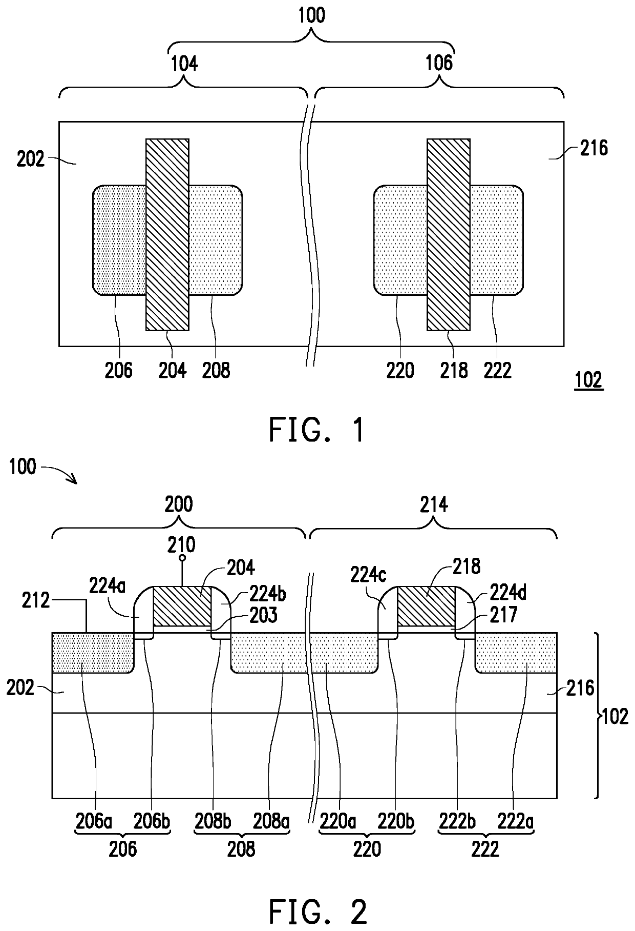
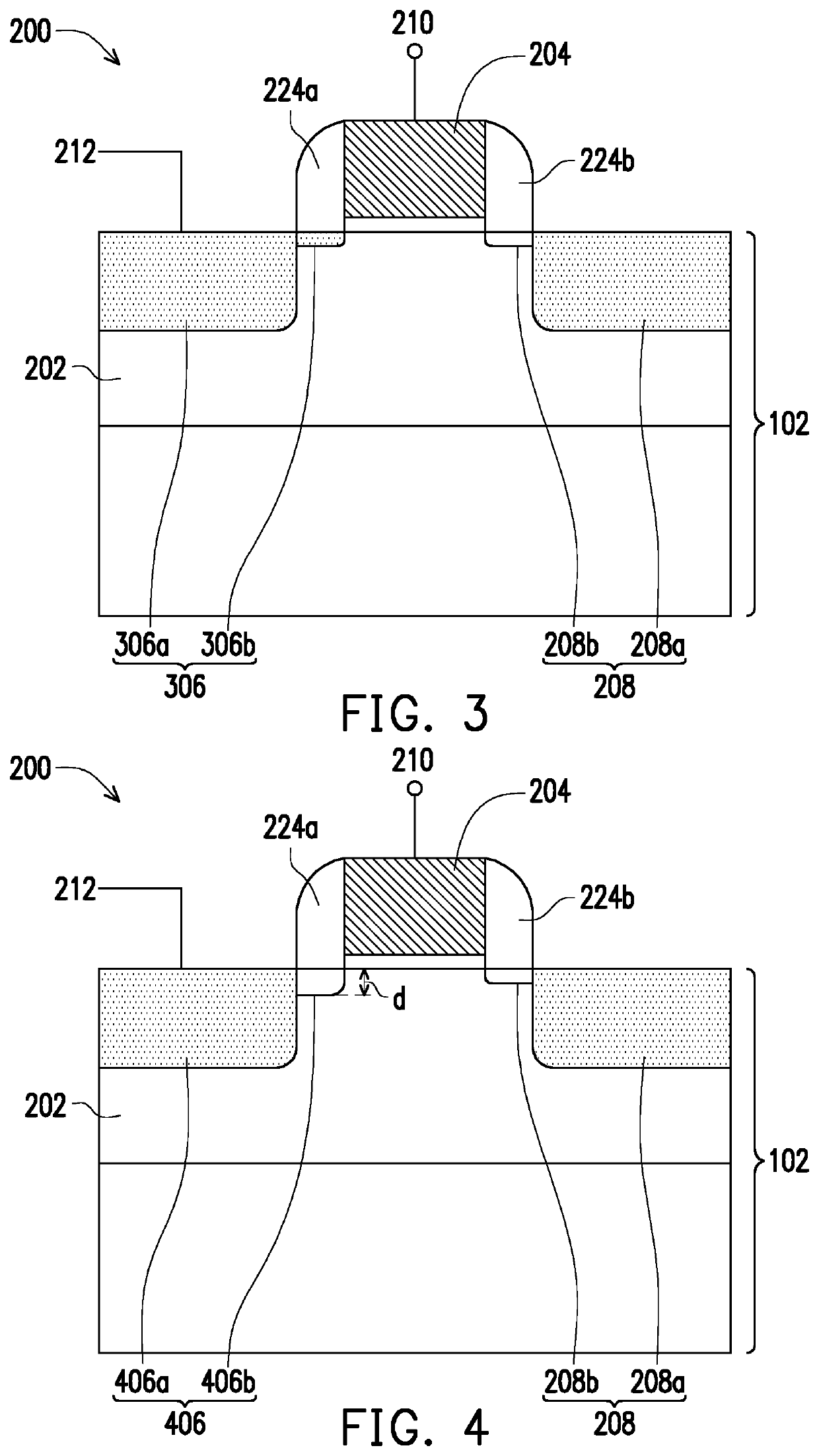
[0021]FIG. 1 is a simplified top view of an integrated circuit according to the disclosure. FIG. 2 is a cross section of the structure of the integrated circuit of FIG. 1.
[0022]Please refer to the diagram shown in FIG. 1 first, wherein an integrated circuit 100, which is represented in the first embodiment, includes an amplifying circuit (e.g., a low-noise amplifying circuit 104) and a logic circuit 106 formed on a substrate 102, and most of the elements of the low-noise amplifying circuit 104 and the logic circuit 106 are omitted. For the detailed structure, please refer to the cross section of FIG. 2.
[0023]Please refer to FIG. 2. The low-noise amplifying circuit 104 of the integrated circuit 100 in the first embodiment includes at least one first transistor 200 formed in the substrate 102. In FIG. 2, the exemplified number of the first transistor 200 is one, but the disclosure is not limited thereto. The material of the substrate 102 is not particularly limited. In some embodiment...
second embodiment
[0041]FIG. 8 is a schematic of a low-noise amplifying circuit in an integrated circuit according to the disclosure.
[0042]Please refer to FIG. 8. A low-noise amplifying circuit 800 in the integrated circuit may include one first transistor. The first transistor of the second embodiment is similar to the various aspects of the first embodiment and is not elaborated. In the low-noise amplifying circuit 800, the first gate of the first transistor is coupled to an analog signal input terminal SIGin. The first source of the first transistor is coupled to a reference voltage terminal. Compared to the operating voltage of the first drain, the reference voltage terminal is a low-voltage or ground, and one passive element 802 (such as a degeneration inductor) may be coupled between the first source of the first transistor and the reference voltage terminal. The first drain of the first transistor is coupled to a supply voltage terminal Vcc that supplies power, and to an analog signal output t...
PUM
 Abstract
Description
Claims
Application Information