Display panel
a display panel and thin film technology, applied in the field of display panels, can solve the problems of reducing the service life of the display panel, and achieve the effects of increasing the bonding force between thin film layers and reducing the service life of the display panel
- Summary
- Abstract
- Description
- Claims
- Application Information
AI Technical Summary
Benefits of technology
Problems solved by technology
Method used
Image
Examples
first embodiment
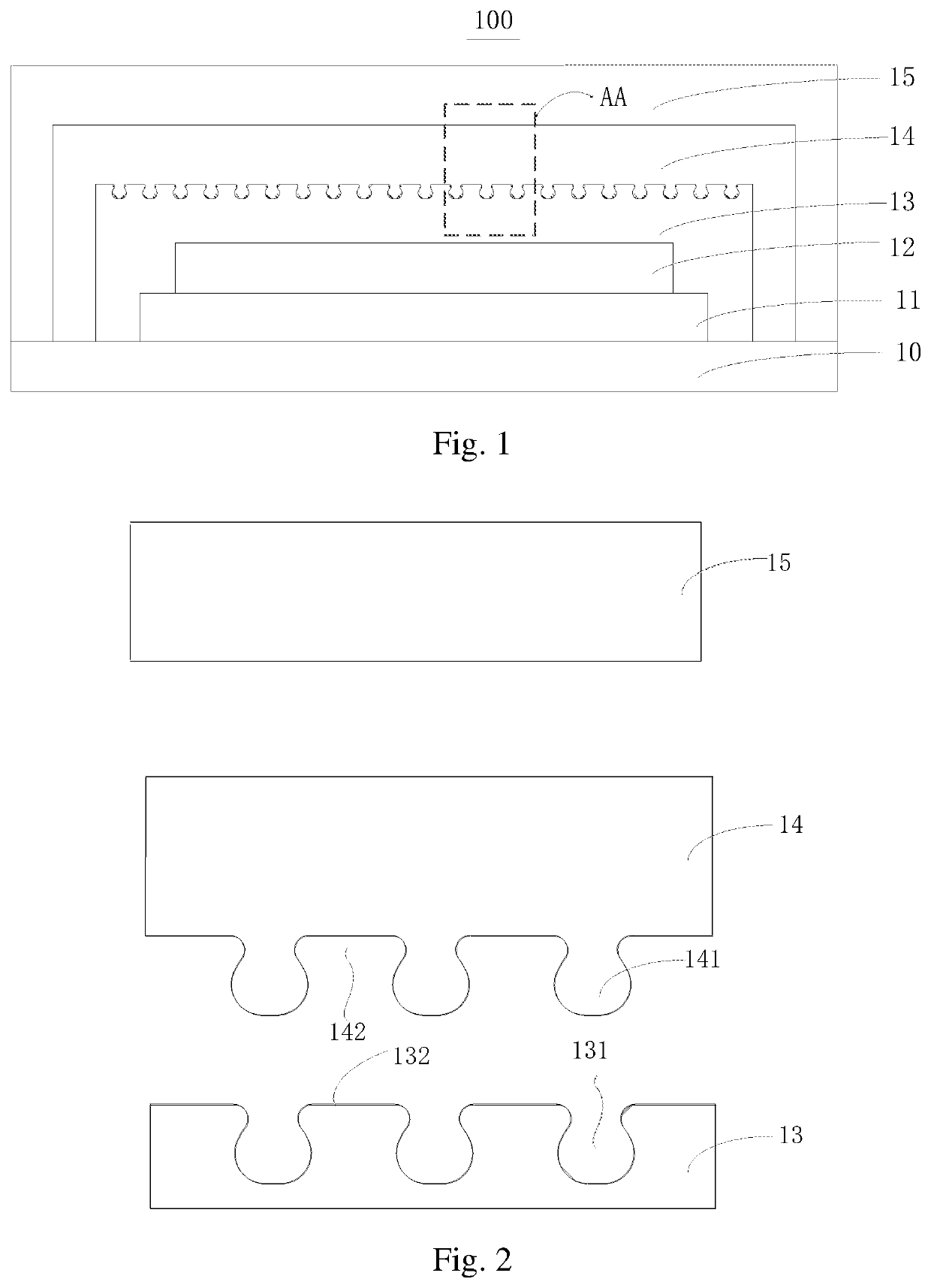
[0035]FIG. 1 is a schematic structural diagram of a display panel according to the present disclosure. As shown in FIG. 1, the display panel 100 may include a substrate 10, a drive layer 11, an organic light emitting layer 12, a first inorganic layer 13, an organic layer 14, and a second inorganic layer 15.
[0036]In this embodiment, the first inorganic layer 13, the organic layer 14, and the second inorganic layer 15 may constitute the encapsulation layer. That is, the encapsulation layer may include multiple layers, i.e., three thin film layers, which are the first inorganic layer 13, the organic layer 14, and the second inorganic layer 15 respectively.
[0037]The drive layer 11 may be disposed on the substrate 10. The organic light emitting layer 12 may be disposed on the drive layer 11. The first inorganic layer 13 may be in contact with the organic light emitting layer 12 and cover the organic light emitting layer 12. The organic layer 14 may cover the first inorganic layer 13. The...
second embodiment
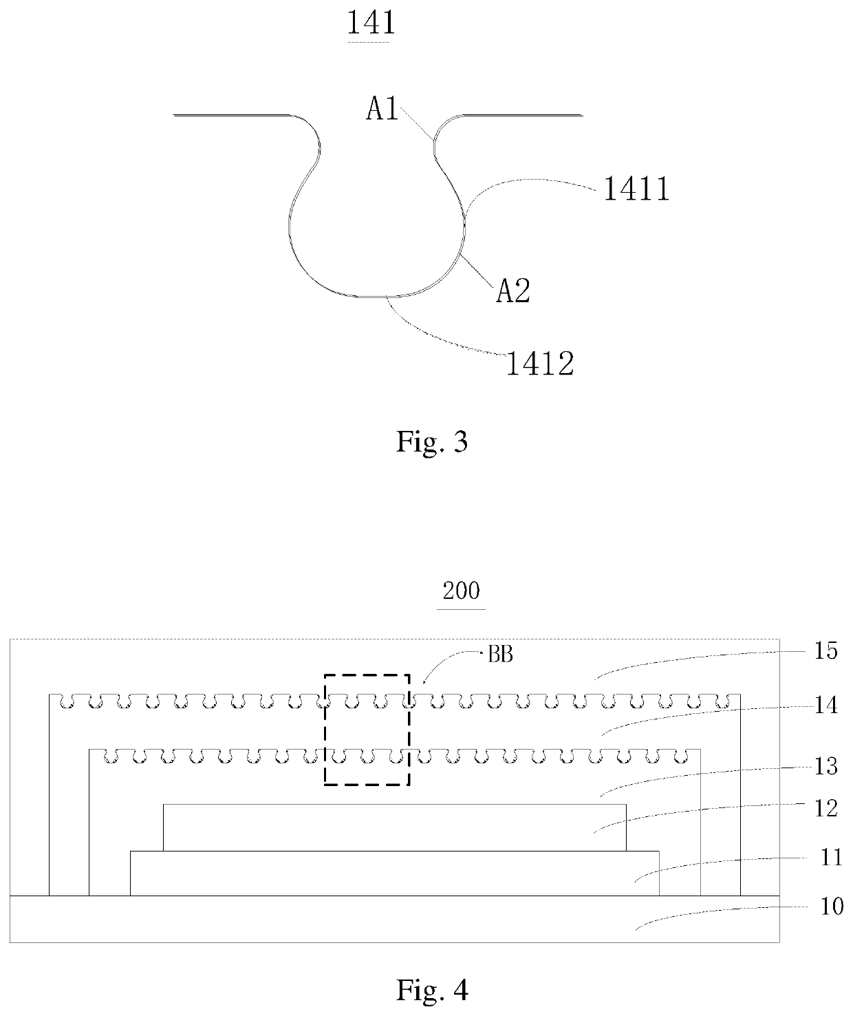
[0047]FIG. 4 is a schematic structural diagram of a display panel 200 according to the present disclosure. FIG. 5 is an explosive schematic structural diagram at BB in the display panel 200 shown in FIG. 4. As shown in FIG. 4 and FIG. 5, the difference between the display panel 200 and the display panel 100 is that: multiple second recesses 143 may be defined at a side face of the organic layer 14 away from the organic light emitting layer 12, multiple second protrusions 151 may be provided on a side face of the second inorganic layer 15 close to the organic light emitting layer 12.
[0048]The second protrusions 151 of the second inorganic layer 15 could be engaged in the second recesses 143 of the organic layer 14, which could enhance the bonding force between the organic layer 14 and the second inorganic layer 15, improve the dynamic bending resistance capability of the display panel 200, and better prevent the encapsulation thin film from peeling.
[0049]The second protrusions 151 ma...
third embodiment
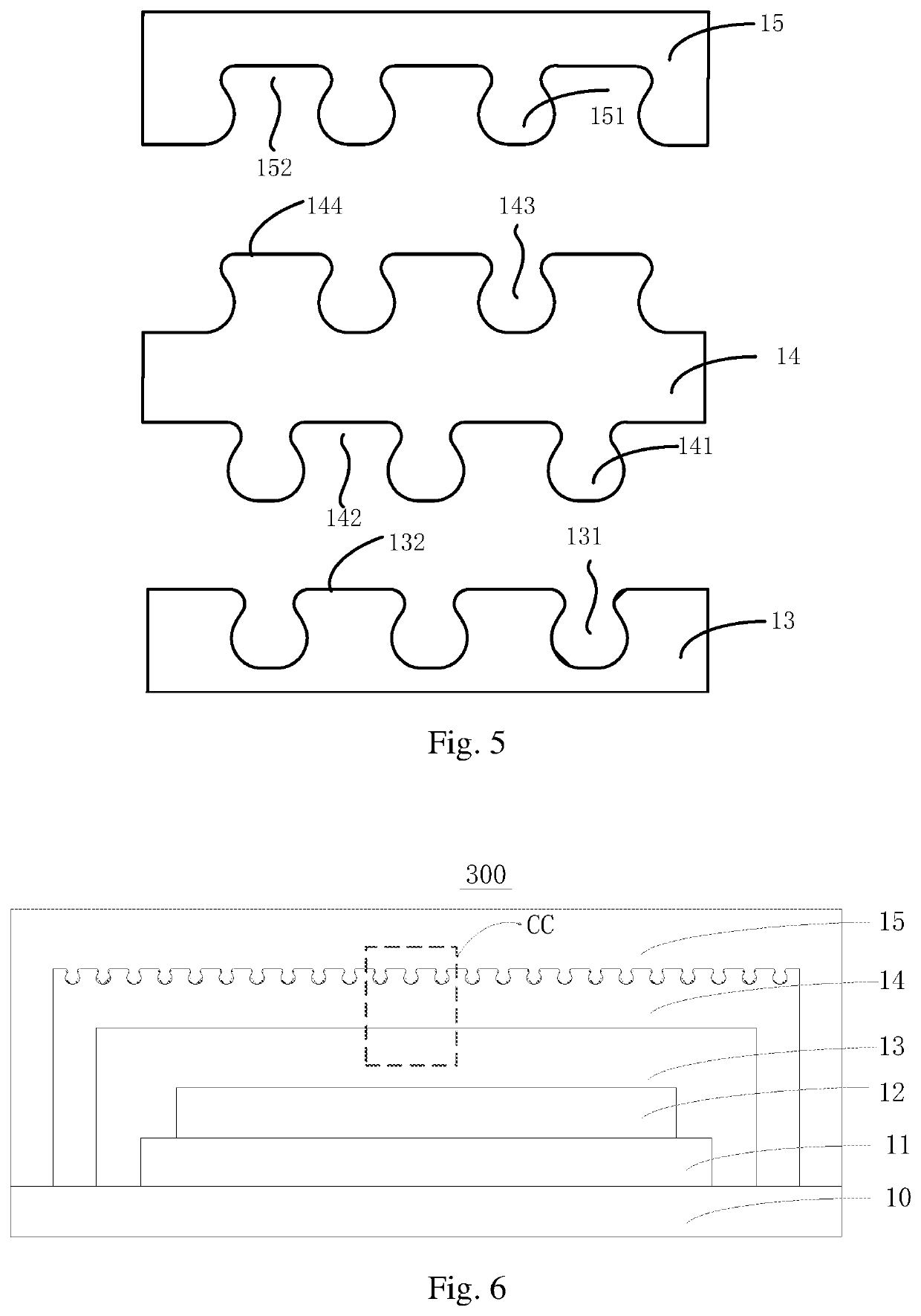
[0059]FIG. 6 is a schematic structural diagram of a display panel 300 according to the present disclosure. FIG. 7 is an explosive schematic structural diagram at CC in the display panel 300 shown in FIG. 6. As shown in FIG. 6 and FIG. 7, the difference between the display panel 300 and the display panel 200 may be that: the first inorganic layer 13 of the display panel 300 does not define the first recesses 131, the organic layer 14 does not include the first protrusions 141. That is, in the display panel 300, the concave-convex engagement may only exist between the second recesses 143 of the organic layer 14 and the second protrusions 151 of the second inorganic layer 15.
[0060]The display panels 300 shown in FIG. 1, FIG. 4 and FIG. 6 is illustrated by an example of an encapsulating layer including three thin film layers, that is an encapsulating layer including a first inorganic layer, an organic layer and a second inorganic layer stacked successively. But this is only schematic. I...
PUM
 Abstract
Description
Claims
Application Information


