Check patentability & draft patents in minutes with Patsnap Eureka AI!

Firmware Boot Implementation Method Based on Flash Chip Simulation

a technology of flash chips and implementation methods, applied in the chip field, can solve problems such as resource waste, circuit complexity and cost increase, and achieve the effects of reducing costs, maximizing resource utilization, and maximizing storage spa

Active Publication Date: 2020-10-15
XIAMEN YEALINK NETWORK TECH
View PDF0 Cites 2 Cited by
  • Summary
  • Abstract
  • Description
  • Claims
  • Application Information

AI Technical Summary

Benefits of technology

The present patent provides a way to simplify the circuitry, save space, and reduce costs of a firmware boot implementation method using Flash chip simulation. By utilizing a Flash chip with a larger storage space and being able to be used by multiple microcontrol units, the method maximizes resource utilization, reduces costs, and simplifies the circuit design.

Problems solved by technology

When the system is relatively complex and has multiple MCUs to work, it is needed to mount the same number of Flash chips outside the MCUs.
In fact, the actual utilization of every Flash chip is not high, and lots of storage space is not utilized, which renders the problems of resources waste, circuit complexity and cost increase, etc.

Method used


Image

  • Firmware Boot Implementation Method Based on Flash Chip Simulation
  • Firmware Boot Implementation Method Based on Flash Chip Simulation
  • Firmware Boot Implementation Method Based on Flash Chip Simulation

Examples


Embodiment Construction

[0021]In the following, the technical solutions in the embodiments of the present disclosure will be clearly and completely described with reference to the drawings in the embodiments of the present disclosure. Apparently, the described embodiments are merely a part of the embodiments of the present disclosure, but not all embodiments. Based on the embodiments of the present disclosure, all other embodiments obtained by a person of ordinary skill in the art without creative efforts shall fall within the protection scope of the present disclosure.

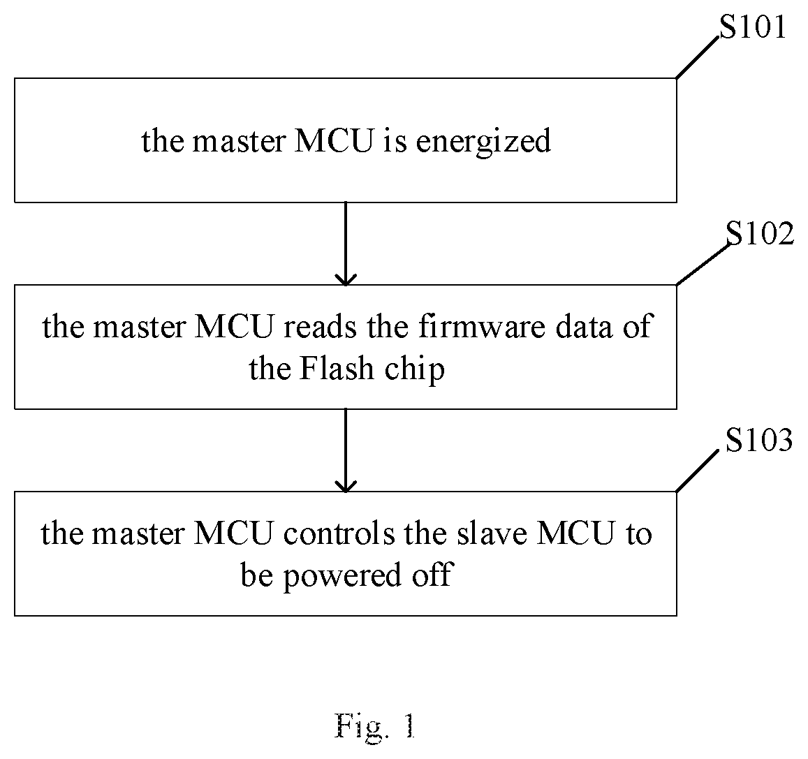
[0022]FIG. 1 is a startup flowchart of the master MCU in the firmware boot implementation method based on Flash chip simulation provided by the embodiments of the prevent disclosure. The startup of the master MCU comprises:

[0023]S101, the master MCU is energized.

[0024]MCU, i.e. Microcontroller Unit, also known as Single Chip Microcomputer or Microcontroller, is a chip-level computer formed by appropriately reducing the frequency and specific...


PUM


Abstract

The embodiments of the present disclosure disclose a firmware boot implementation method based on Flash chip simulation, the method comprising: when there are at least two MCUs, one of the MCUs is selected as a master MCU and each remaining MCU is as slave MCU which is connected with the master MCU respectively, and the master MCU is connected with a Flash chip; when the master MCU is started, the master MCU is started by reading firmware data in the Flash chip; when the slave MCU is started, the master MCU controls the slave MCU to be powered on, and the slave MCU sends a request for reading the firmware data to the master MCU; the master MCU transmits the request to the Flash chip, and transmits the firmware data returned by the Flash chip to the slave MCU, so as to start the slave MCU.

Description

CROSS-REFERENCE TO RELATED APPLICATIONS[0001]The present application claims the benefit of Chinese Patent Application No. 201910288563.8 filed on Apr. 11, 2019, the contents of which are hereby incorporated by reference.FIELD OF THE DISCLOSURE[0002]The present disclosure relates to chip area and is more particularly concerned with a firmware boot implementation method based on Flash chip simulation.BACKGROUND OF THE DISCLOSURE[0003]There are two ways to start MCU (Microcontroller Unit), one is to operate directly from the firmware on the MCU, and the other is to operate after dynamically booting and loading firmware. The traditional way is to mount a Flash chip outside the MCU. When the system is relatively simple and only has one MCU, it is needed to mount one Flash chip. When the system is relatively complex and has multiple MCUs to work, it is needed to mount the same number of Flash chips outside the MCUs. Since one MCU is mounted with one Flash chip, the system loaded with mult...

Claims


Application Information

Patent Timeline
Patent Type & Authority Applications(United States)
IPC IPC(8): G06F9/4401G06F3/06G06F1/28
CPCG06F9/4406G06F3/0659G06F1/28G06F3/0604G06F3/0679G06F9/4403G06F9/4408
Inventor FENG, WANJIANZHANG, LIANCHANGLUO, ZHAOYANGZENG, BINGYANG
Owner XIAMEN YEALINK NETWORK TECH
Features
  • R&D
  • Intellectual Property
  • Life Sciences
  • Materials
  • Tech Scout
  • Unparalleled Data Quality
  • Higher Quality Content
  • 60% Fewer Hallucinations
Learn More