Eureka AIR delivers breakthrough ideas for toughest innovation challenges, trusted by R&D personnel around the world.

Anti-fuse structure and method for fabricating same, as well as semiconductor device

a technology of anti-fuse and anti-oxidation layer, which is applied in the direction of semiconductor devices, semiconductor/solid-state device details, electrical apparatus, etc., can solve the problems of increasing the difficulty of high-voltage transistor formation, and achieve the effects of reducing power consumption, reducing the difficulty of forming the fuse oxide layer, and reducing the difficulty of forming the high-voltage transistor

Active Publication Date: 2020-11-12
CHANGXIN MEMORY TECH INC
View PDF0 Cites 0 Cited by
  • Summary
  • Abstract
  • Description
  • Claims
  • Application Information

AI Technical Summary

Benefits of technology

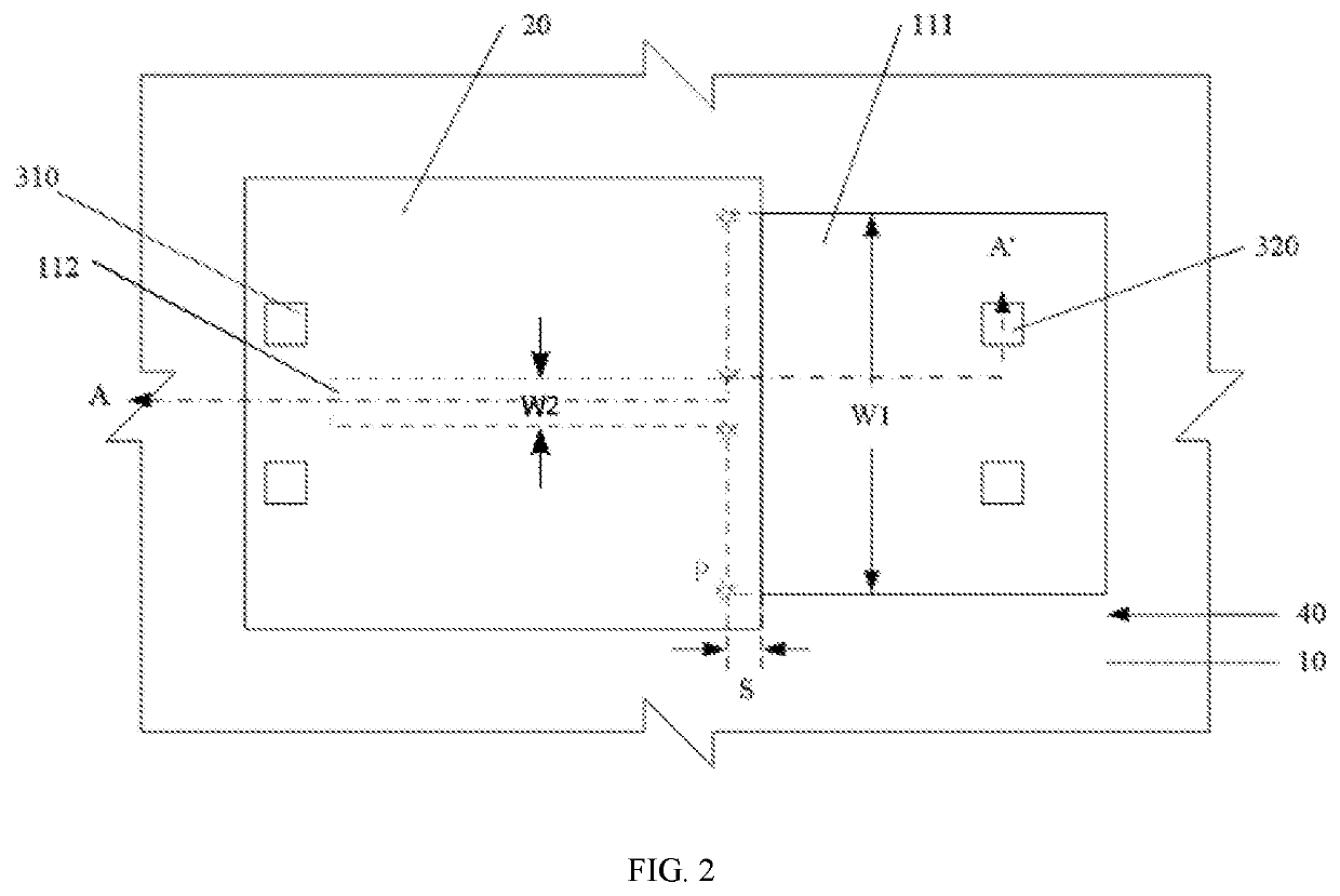
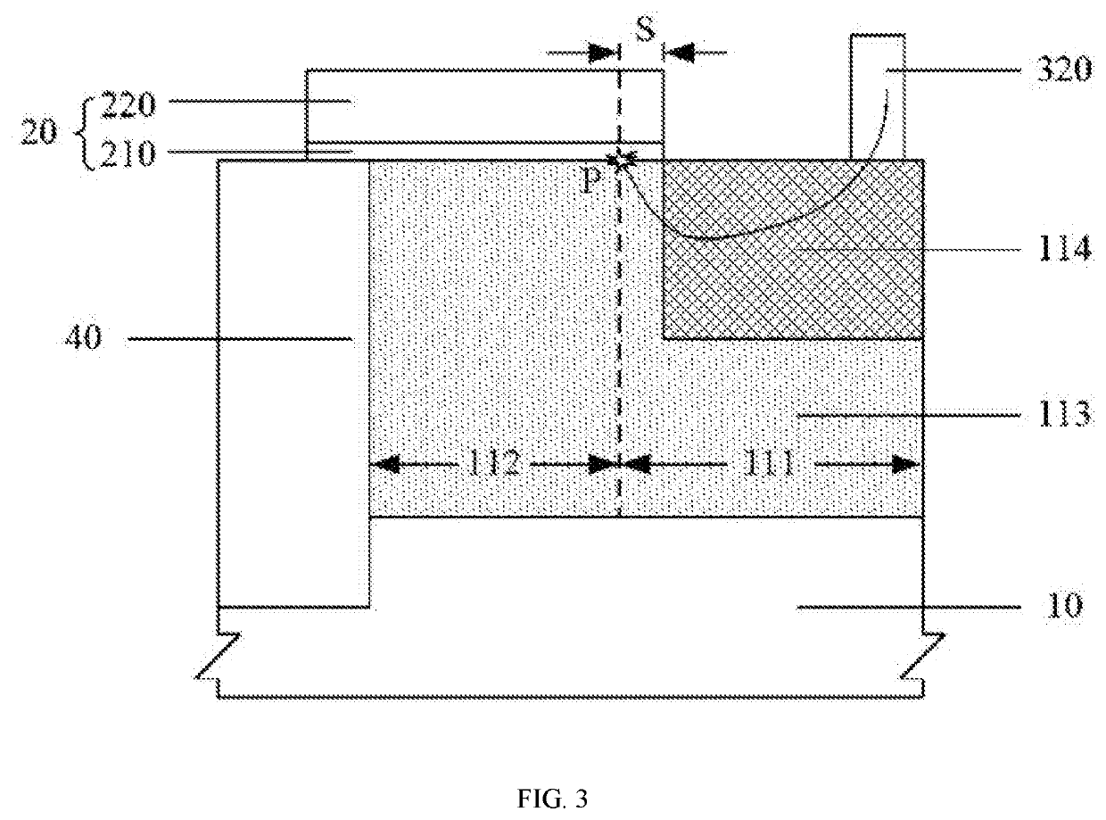
This patent relates to an anti-fuse structure and a method for making the structure. The structure has wide and narrow portions and a fuse oxide layer covering the narrow portion and a portion of the wide portion. The fuse oxide layer can be broken down easily, which results in lower power consumption and simplifies the peripheral circuit design. When used in memory devices, the structure allows for higher memory capacity.

Problems solved by technology

As the feature size of semiconductor technology continues to shrink, the formation of such high-voltage transistors will become increasingly challenging.

Method used


Image

  • Anti-fuse structure and method for fabricating same, as well as semiconductor device
  • Anti-fuse structure and method for fabricating same, as well as semiconductor device
  • Anti-fuse structure and method for fabricating same, as well as semiconductor device

Examples


Embodiment Construction

[0054]Anti-fuse structures, methods for fabricating them and semiconductor devices according to the present disclosure will be described below in greater detail with reference to the accompanying schematics, which illustrate preferred embodiments of the disclosure. Those skilled in the art can make changes to the disclosure herein while still obtaining the beneficial results thereof. Therefore, the following description shall be construed as being intended to be widely known by those skilled in the art rather than as limiting the disclosure.

[0055]Any layer (or film), region, pattern or structure described hereinafter as being “on” or “over” a substrate, another layer (or film), another region, a pad and / or another pattern may be either in direct contact with the other substrate, layer, region, pad and / or pattern, or indirectly on the other substrate, layer, region, pad and / or pattern with one or more layers inserted therebetween. In addition, any layer described hereinafter as being...


PUM

PropertyMeasurementUnit
pressureaaaaaaaaaa
thicknessaaaaaaaaaa
widthaaaaaaaaaa

Abstract

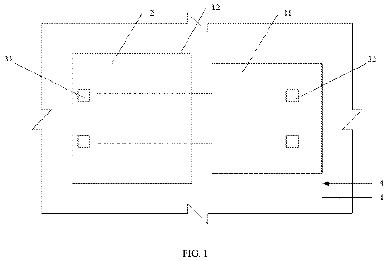
An anti-fuse structure, a method for fabricating the anti-fuse structure, and a semiconductor device are disclosed. The anti-fuse structure includes a semiconductor substrate, a fuse oxide layer, a gate material layer, a first electrode and a second electrode. An active area is defined on the semiconductor substrate by an isolation structure. The active area includes a wide portion and a narrow portion connected to each other. The fuse oxide layer is located on the semiconductor substrate, covers the narrow portion and extends to cover a first part of the wide portion. The gate material layer is formed on the fuse oxide layer. The first electrode is formed on and electrically connected to the gate material layer, while the second electrode is formed on and electrically connected to a second part of the wide portion not covered by the fuse oxide layer.

Description

CROSS-REFERENCE TO RELATED APPLICATIONS[0001]This application is a continuation application of International Patent Application No.: PCT / CN2018 / 125298, filed on Dec. 29, 2018, which claims priority to China Patent Application No. 201711488681.0, filed with the China Patent Office on Dec. 29, 2017 and entitled “ANTI-FUSE STRUCTURE AND METHOD FOR FABRICATING SAME, AS WELL AS SEMICONDUCTOR DEVICE.” The above-referenced applications are incorporated herein by reference in their entirety.TECHNICAL FIELD[0002]The present disclosure relates to the field of semiconductor technology and, in particular, to an anti-fuse structure, a method for fabricating the anti-fuse structure and a semiconductor device.BACKGROUND[0003]Fuses and anti-fuses are widely used in existing integrated circuits (ICs) to selectively connect a component to other parts of the circuit or disconnect the component from the other parts of the circuit so as to provide logic operations. A fuse can be activated (i.e., melted,...

Claims


Application Information

Patent Timeline
Patent Type & Authority Applications(United States)
IPC IPC(8): H01L23/525H01L23/528H01L21/311
CPCH01L21/311H01L23/5283H01L23/5252
Inventor LIU, CHIH CHENG
Owner CHANGXIN MEMORY TECH INC
Why Eureka
Eureka Blog
Learn More