
Semiconductor device and manufacturing method thereof

a technology of semiconductor devices and manufacturing methods, applied in semiconductor devices, semiconductor/solid-state device details, capacitors, etc., can solve problems such as the possibility of hitting through the storage capacitor and bit lin

Active Publication Date: 2020-12-10
WINBOND ELECTRONICS CORP
View PDF0 Cites 5 Cited by
  • Summary
  • Abstract
  • Description
  • Claims
  • Application Information

AI Technical Summary

Benefits of technology

The present disclosure provides a DRAM device and manufacturing method that avoids punch through between the storage capacitors and bit lines. By using a conductive ring to protect elements and enlarge the contact area, charge punch through from the storage capacitor to the underlying bit line can be prevented, improving the reliability of the semiconductor device. The conductive ring can be formed by a self-aligning patterning process without needing an additional photolithography process.

Problems solved by technology

However, such shift of the storage capacitors may result in overlap between the storage capacitors and bit lines, and punch through problem between the storage capacitors and bit lines may occur.

Method used


Image

  • Semiconductor device and manufacturing method thereof
  • Semiconductor device and manufacturing method thereof
  • Semiconductor device and manufacturing method thereof

Examples


Embodiment Construction

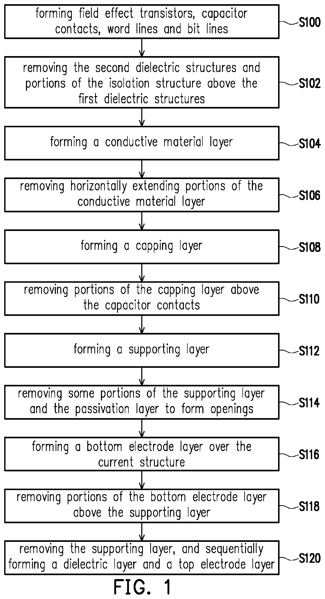
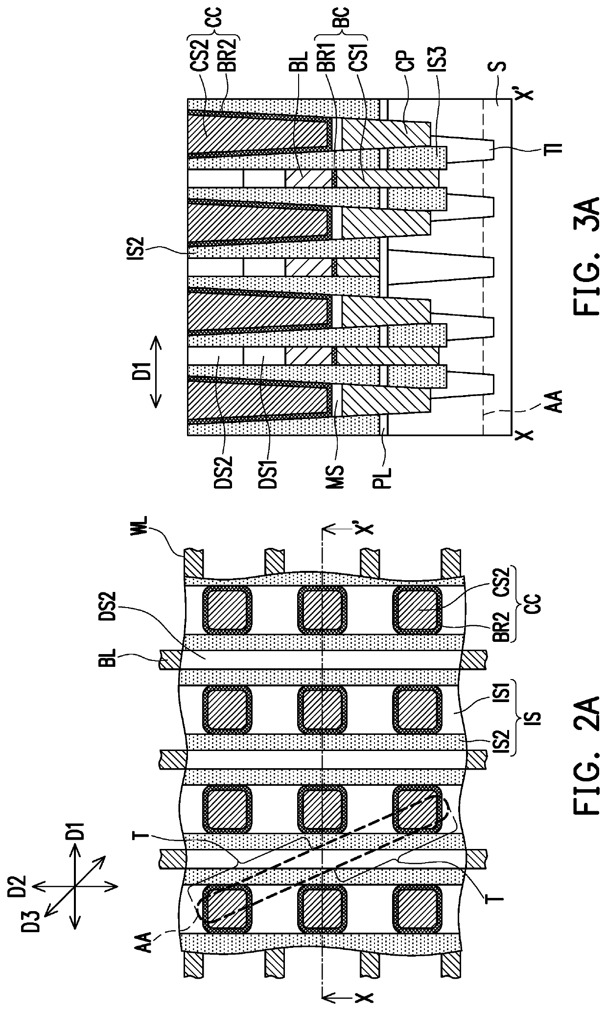
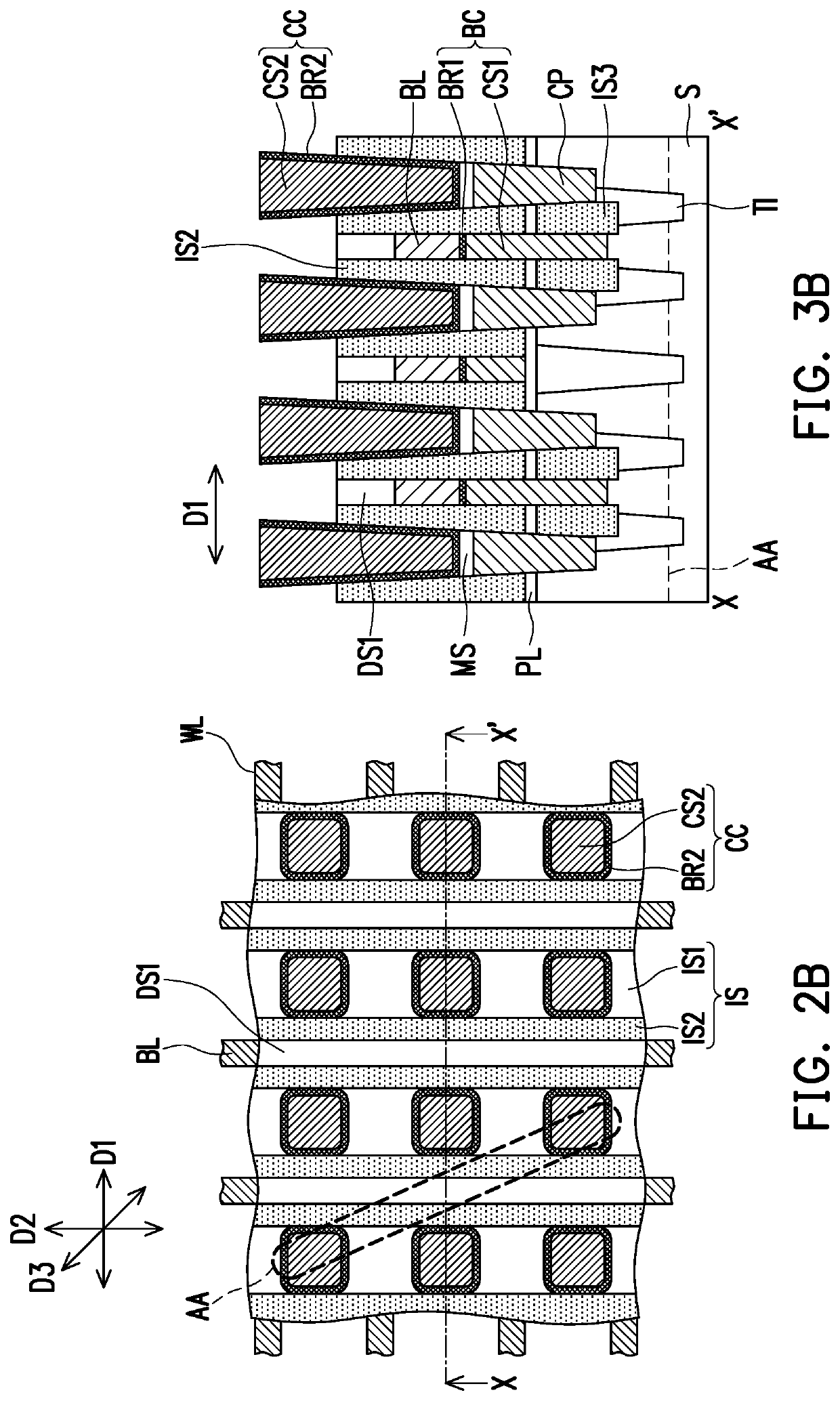
[0012]FIG. 1 is a process flow of a manufacturing method of a semiconductor device according to some embodiments of the present disclosure. FIG. 2A through FIG. 2K are schematic top views of structures at various stages during the manufacturing method of the memory device illustrate in FIG. 1. FIG. 3A through FIG. 3K are schematic cross-sectional views along the lines X-X′ shown in FIG. 2A through FIG. 2K, respectively.

[0013]Referring to FIG. 1, FIG. 2A, step S100 is performed, and field effect transistors T, capacitor contacts CC, word lines WL and bit lines BL are formed. In some embodiments, the word lines WL extend along a first direction D1, whereas the bit lines BL extend along a second direction D2 that is intersected with the first direction D1. For instance, the first direction D1 may be perpendicular to the second direction D2. At least one of the field effect transistors T is formed within the span of an active region AA. For instance, as shown in FIG. 2A, two field effec...


PUM

PropertyMeasurementUnit
angleaaaaaaaaaa
conductiveaaaaaaaaaa
dielectricaaaaaaaaaa

Abstract

A semiconductor device and a manufacturing method are provided. The semiconductor device includes an active region, a bit line, a capacitor contact, a conductive ring and a storage capacitor. The active region is formed in a substrate. The bit line and the capacitor contact are disposed over the substrate and electrically connected with the active region. The bit line is laterally separated from the capacitor contact, and a top surface of the bit line is lower than a top surface of the capacitor contact. An upper portion of the capacitor contact is surrounded by the conductive ring. The storage capacitor is disposed over and in electrical contact with the capacitor contact and the conductive ring.

Description

BACKGROUNDTechnical Field[0001]The present disclosure relates to a semiconductor device and a manufacturing method thereof, and particularly, to a dynamic random access memory (DRAM) device and a manufacturing method thereof.Description of Related Art[0002]Dynamic random access memory (DRAM) is a widely used volatile read / write semiconductor memory device. A memory cell of a DRAM integrated circuit includes a field effect transistor and a storage capacitor. A gate of the field effect transistor is connected to a word line, and source and drain of the field effect transistor are connected to a bit line and the storage capacitor. In order to increase the area of the storage capacitor (i.e., the capacitance of the storage capacitor) without excessively reducing the spacing between adjacent storage capacitors in the DRAM integrated circuit, the storage capacitors may be shifted from the underlying capacitor contacts by a certain distance. However, such shift of the storage capacitors ma...

Claims


Application Information

Patent Timeline
Patent Type & Authority Applications(United States)
IPC IPC(8): H01L27/108H01L49/02H01L23/31H01L21/3213H01L21/311
CPCH01L21/31144H01L28/60H01L21/32133H01L27/10885H01L23/3171H01L27/10855H01L27/10814H01L28/90H10B12/315H10B12/033H10B12/0335H10B12/482
Inventor IKEDA, NORIAKI
Owner WINBOND ELECTRONICS CORP
Learn More