Plasma processing apparatus and plasma processing method

a processing apparatus and plasma technology, applied in the direction of electrical apparatus, basic electric elements, electric discharge tubes, etc., can solve the problems of inability to achieve optimal treatment, unsatisfactory minute step shape, and delay of about 1 second, and achieve small machine difference in the application time of radio frequency power, high shape controllability, and the effect of small machine differen

Active Publication Date: 2020-12-24
HITACHI HIGH-TECH CORP
View PDF0 Cites 3 Cited by
  • Summary
  • Abstract
  • Description
  • Claims
  • Application Information

AI Technical Summary

Benefits of technology

[0041]a control device configured to control, when the first radio frequency power source is controlled based on a change in a plasma impedance, which is generated when a first gas that is a gas for a first step is switched to a second gas that is a gas for a second step, such that the first radio frequency power is changed from a value of the first radio frequency power in the first step to a value of the first radio frequency power in the second step, a supply time of the second gas by using a first time and a second time such that a supply time of the first radio frequency power in the second step is substantially equal to a time of the second step, in which
[0099]Problems, configurations, and effects other than those described above will be clarified by the following description of embodiments.

Problems solved by technology

When an etching treatment is performed while alternately performing etching and forming the protective film by using the gas pulse method, a minute step shape referred to as scalloping is formed on a side surface of a processed hole after the etching, but this minute step shape is undesirable when forming the semiconductor device.
However, during a time period from a time when the flow rate signal is given to the gas supply device to a time when the gas is introduced into the processing chamber, a delay about 1 second is generated by influences such as a response time of the gas supply device, or pressure and a gas flow in the processing chamber, gas pipes and a shower plate.
This is because if such control is not performed, a time gap that cannot be ignored is generated between a timing of introducing the gas of a process for etching or forming the protective film in the processing chamber and a timing of controlling process parameters such as a bias and a power for generating the plasma to values suitable for each process, so that optimal treatment will not be implemented.

Method used


Image

  • Plasma processing apparatus and plasma processing method
  • Plasma processing apparatus and plasma processing method
  • Plasma processing apparatus and plasma processing method

Examples


Embodiment Construction

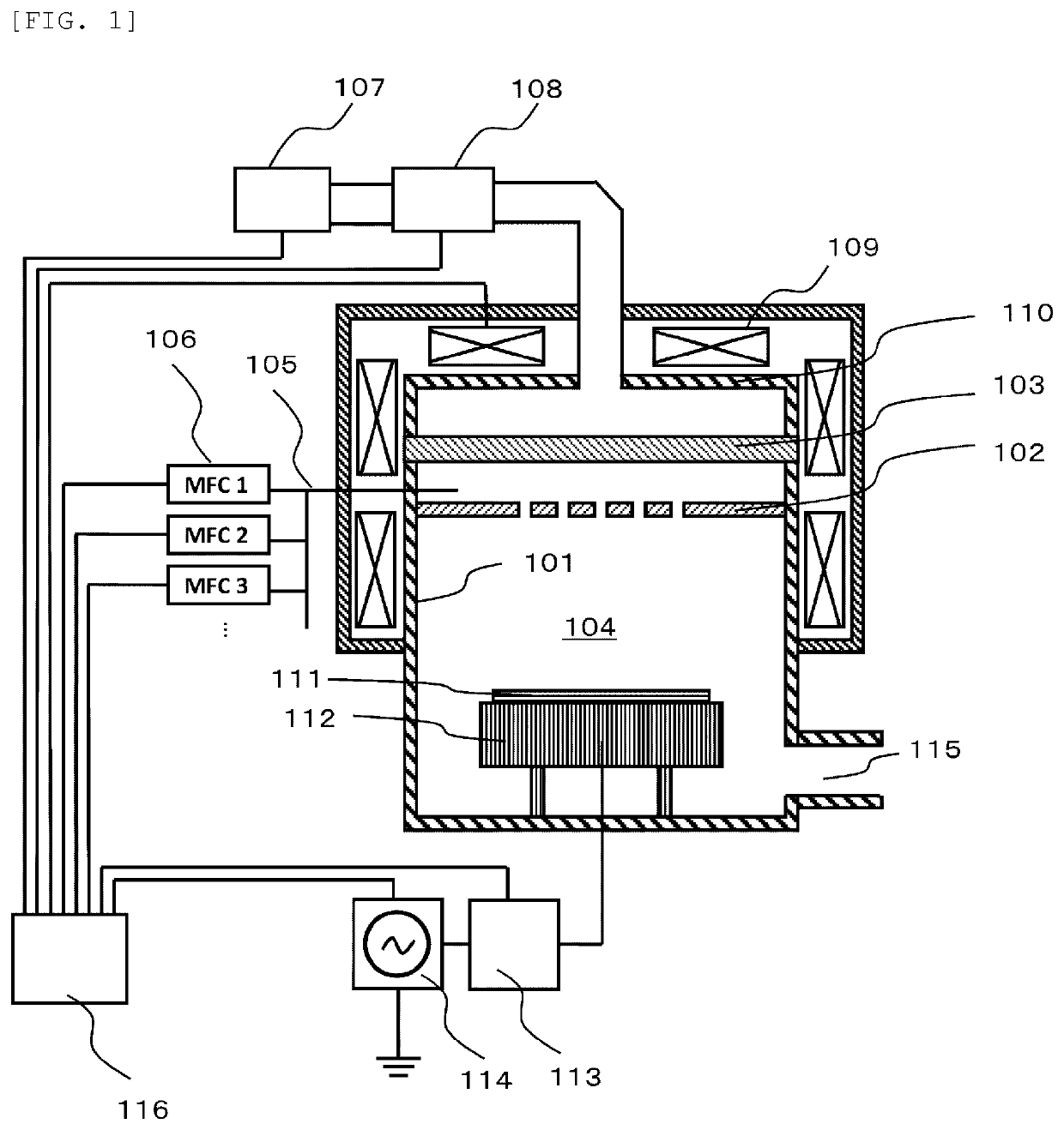
[0104]Hereinafter, an embodiment of the invention is described with reference to the drawings. FIG. 1 is a longitudinal sectional view illustrating an outline of an overall configuration of a plasma processing apparatus according to the present embodiment of the invention. A shower plate 102 for introducing an etching gas into a vacuum vessel 101 and a dielectric window 103 for air tightly sealing an upper portion of a processing chamber are disposed on an upper portion of the vacuum vessel 101 to constitute a processing chamber 104. A plurality of gas supply devices (MFC) 106 are connected to the shower plate 102 via a gas pipe 105, and each gas supply device 106 is respectively connected to a source (not illustrated) of a treatment gas, such as SF6 gas, O2 gas, or the like, for performing a plasma etching treatment.

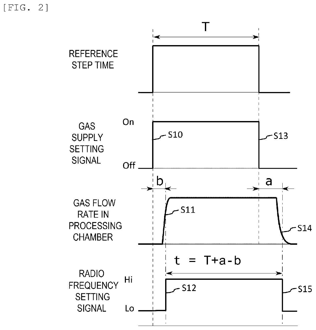
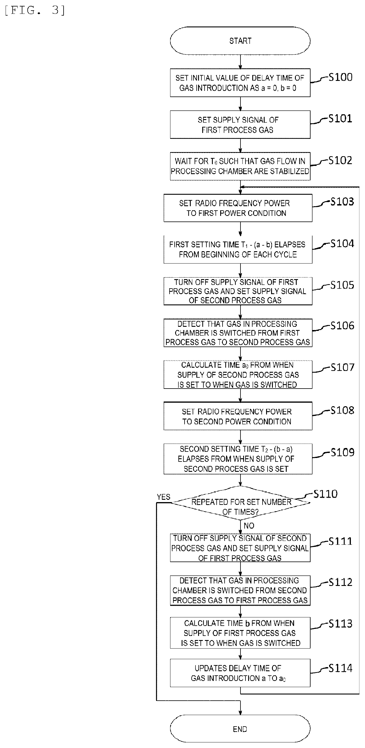
[0105]A first process gas (etching gas) for performing an etching treatment with the plurality of gas supply devices and a second process gas (deposition gas) for perfo...


PUM


Abstract

A plasma processing apparatus, including a processing; a first radio frequency power source; a sample stage on which the sample is placed; a second radio frequency power; and a control device configured to control, when the second radio frequency power source is controlled based on a change in a plasma impedance, which is generated when a first gas that is a gas for a first step is switched to a second gas that is a gas for a second step, such that the second radio frequency power is changed from a value of the second radio frequency power in the first step to a value of the second radio frequency power in the second step, and a supply time of the first gas such that a supply time of the second radio frequency power in the first step is substantially equal to a time of the first step.

Description

TECHNICAL FIELD[0001]The present invention relates to a plasma processing apparatus and a plasma processing method.BACKGROUND ART[0002]In a manufacturing process of a semiconductor device, there is a demand for miniaturization and integration of components included in the semiconductor device. For example, in an integrated circuit and a nanoelectronic mechanical system, a nanoscale structure is further promoted.[0003]In the manufacturing process of the semiconductor device, a lithography technique is usually used to forma fine pattern. In this technique, a pattern of a device structure is applied on a resist layer, and a substrate exposed by the pattern on the resist layer is selectively etched and removed. In subsequent treatment processes, if another material is deposited in an etching region, the integrated circuit can be formed.[0004]Incidentally, in an etching process of transferring a mask shape on a lower layer film, relatively higher shape controllability is required. For ex...

Claims


Application Information

Patent Timeline
Patent Type & Authority Applications(United States)
IPC IPC(8): H01L21/3065H01L21/67H01J37/32
CPCH01L21/30655H01J2237/3343H01J37/321H01J37/32715H01J37/32174H01L21/67069H01J37/32449H01L21/3065H01J37/32009
Inventor SONODA, YASUSHI
Owner HITACHI HIGH-TECH CORP
Why Eureka
Try Eureka