

Semiconductor device and method for manufacturing same
- Summary
- Abstract
- Description
- Claims
- Application Information
AI Technical Summary
Benefits of technology
Problems solved by technology
Method used
Image

Examples
Embodiment Construction
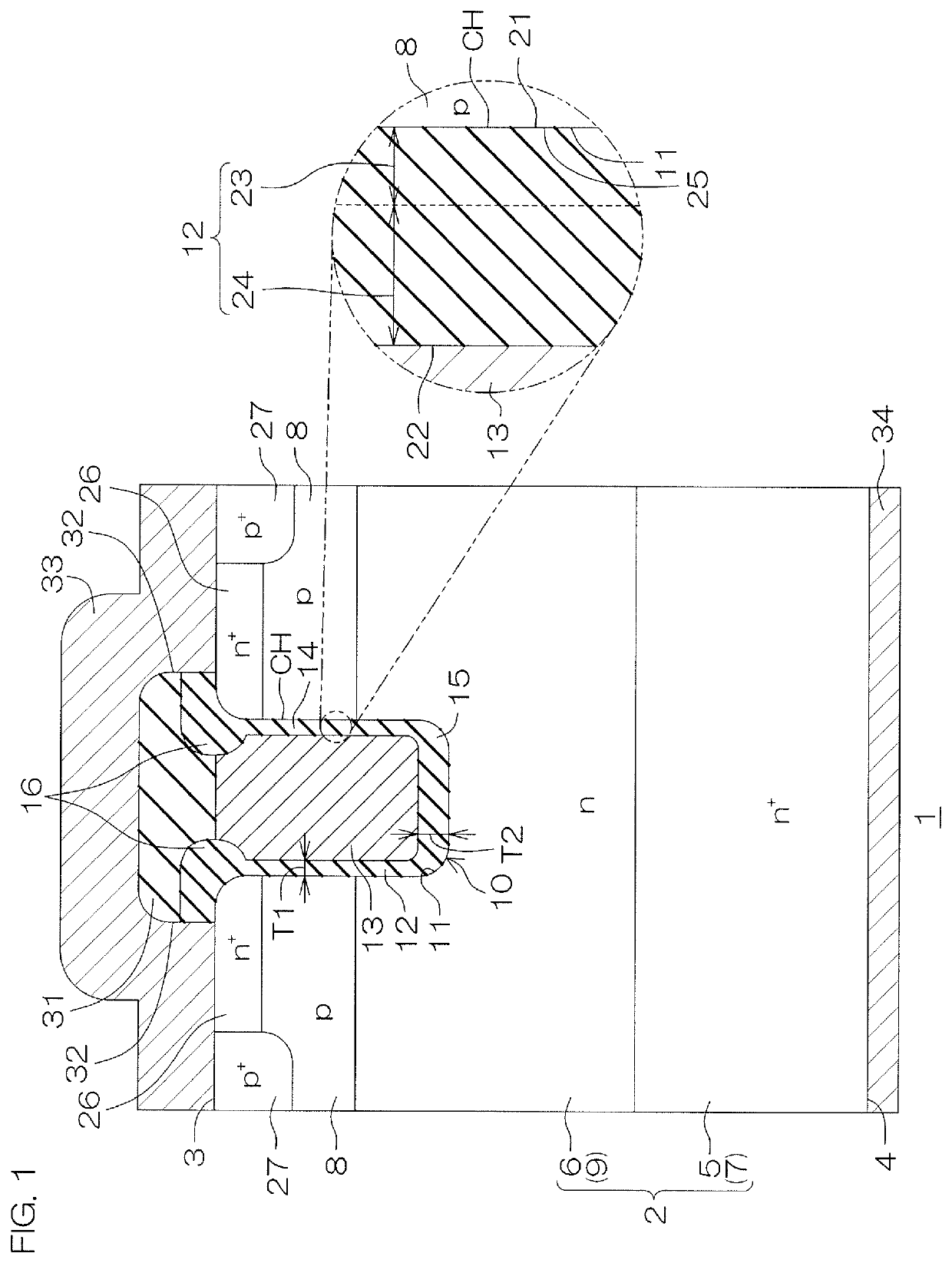
[0049]FIG. 1 is a cross-sectional view showing a region in which a MISFET is formed in a semiconductor device 1 according to a first preferred embodiment of the present invention.
[0050]The semiconductor device 1 has a basic form including a trench-gate type MISFET (Metal Insulator Semiconductor Field Effect Transistor). The semiconductor device 1 includes an n type SiC semiconductor layer 2 to which an n type impurity is added. The SiC semiconductor layer 2 is made of 4H-SiC monocrystal in the present preferred embodiment. The n type impurity of the SiC semiconductor layer 2 may be N (nitrogen), As (arsenic), or P (phosphorus).
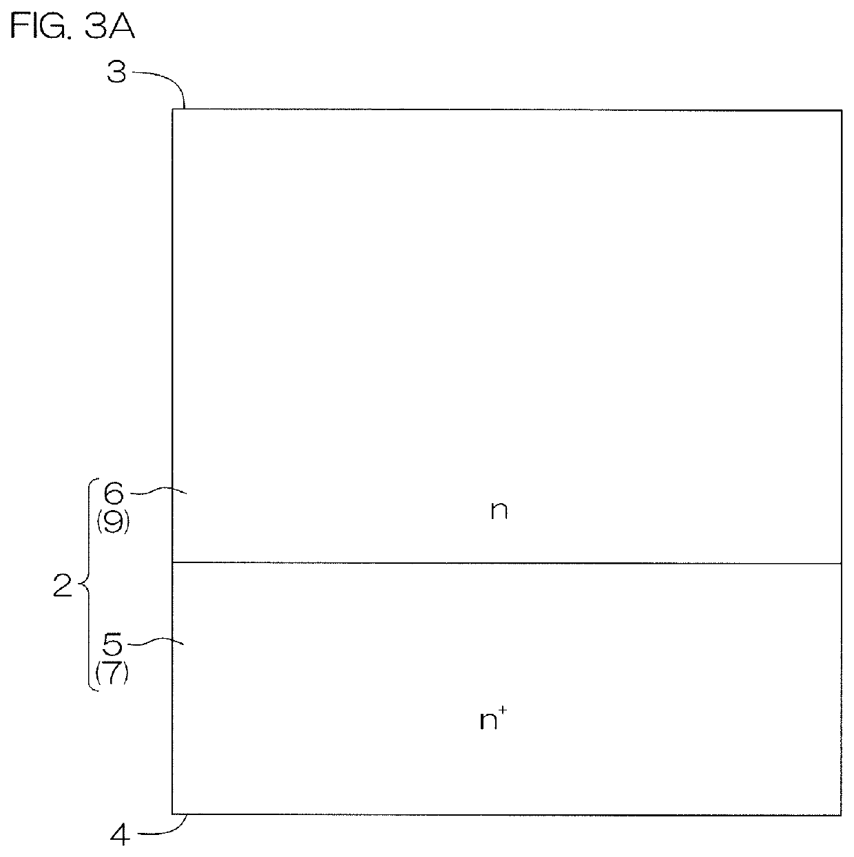
[0051]The SiC semiconductor layer 2 includes a first main surface 3 on one side and a second main surface 4 on the other side. The first main surface 3 and the second main surface 4 may each have an off-angle that is tilted at an angle of 10° or less in a direction with respect to a [0001] plane of the 4H-SiC monocrystal. The off-angle is also an angle betwee...
PUM
 Abstract
Description
Claims
Application Information