
Semiconductor crystal growth apparatus

Inactive Publication Date: 2021-01-14
ZING SEMICON CORP
View PDF0 Cites 0 Cited by
  • Summary
  • Abstract
  • Description
  • Claims
  • Application Information

AI Technical Summary

Benefits of technology

The semiconductor crystal growth device of the present invention regulates the calorific value and compensates for the asymmetry of the silicon melt flow caused by the applied horizontal magnetic field. It reduces the influence of melt temperature fluctuations and regulates the temperature distribution of the silicon melt below the interface between the silicon ingot and the silicon melt, thereby improving the uniformity of the crystal growth rate and the quality of the crystal pulling.

Problems solved by technology

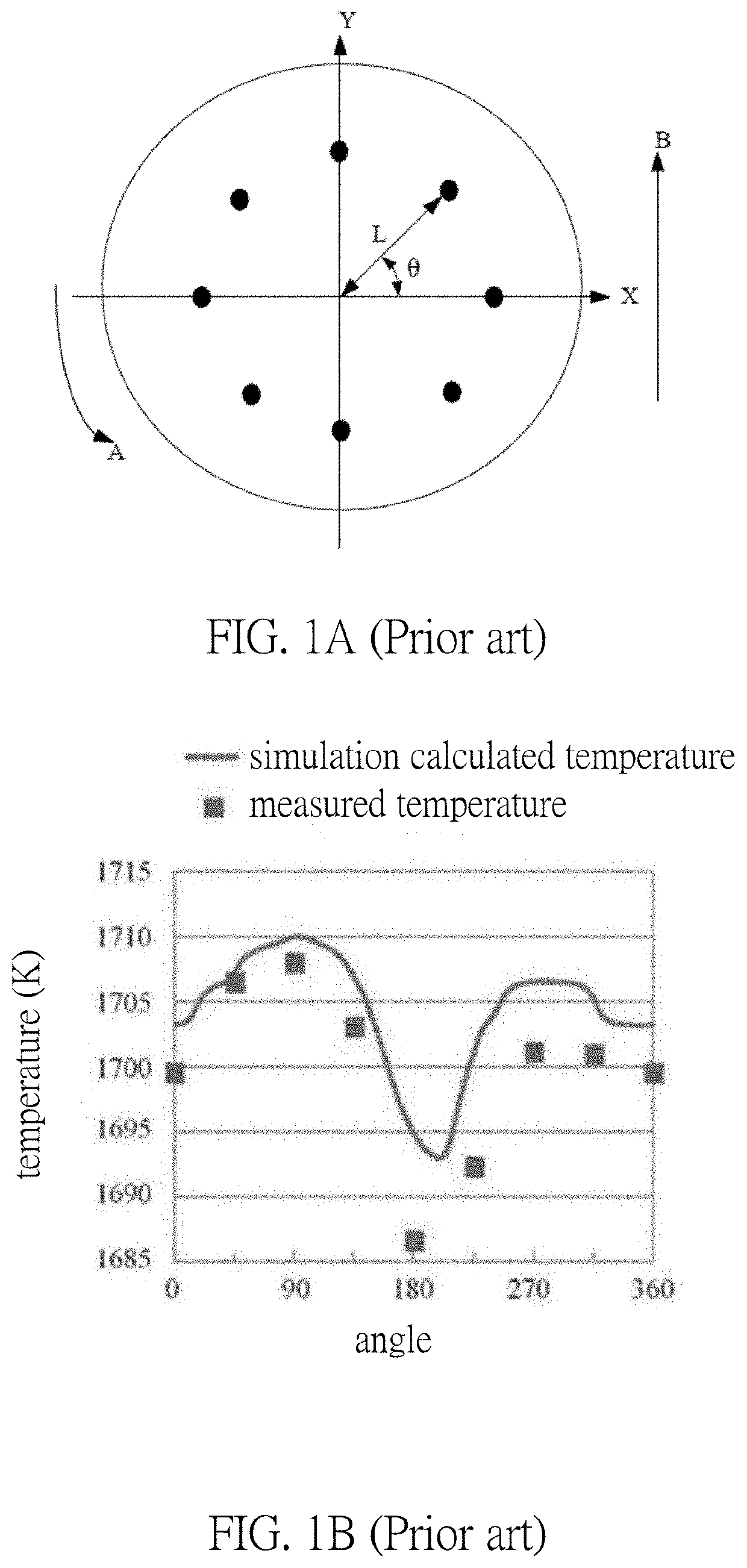
Therefore, the crystallization speed PS of the crystal in the circumferential angle direction fluctuates periodically, which is not conducive to controlling the quality of crystal growth.

Method used


Image

  • Semiconductor crystal growth apparatus
  • Semiconductor crystal growth apparatus
  • Semiconductor crystal growth apparatus

Examples


Embodiment Construction

[0031]The embodiments of the present invention are described below by way of specific examples, and those skilled in the art can readily understand other advantages and effects of the present invention from the disclosure of the present disclosure. The present invention may be embodied or applied in various other specific embodiments, and various modifications and changes can be made without departing from the spirit and scope of the invention.

[0032]In the following description, while the invention will be described in conjunction with various embodiments, it will be understood that these various embodiments are not intended to limit the invention. On the contrary, the invention is intended to cover alternatives, modifications and equivalents, which may be comprised within the scope of the invention as construed according to the Claims. Furthermore, in the following detailed description of various embodiments in accordance with the invention, numerous specific details are set forth ...


PUM


Abstract

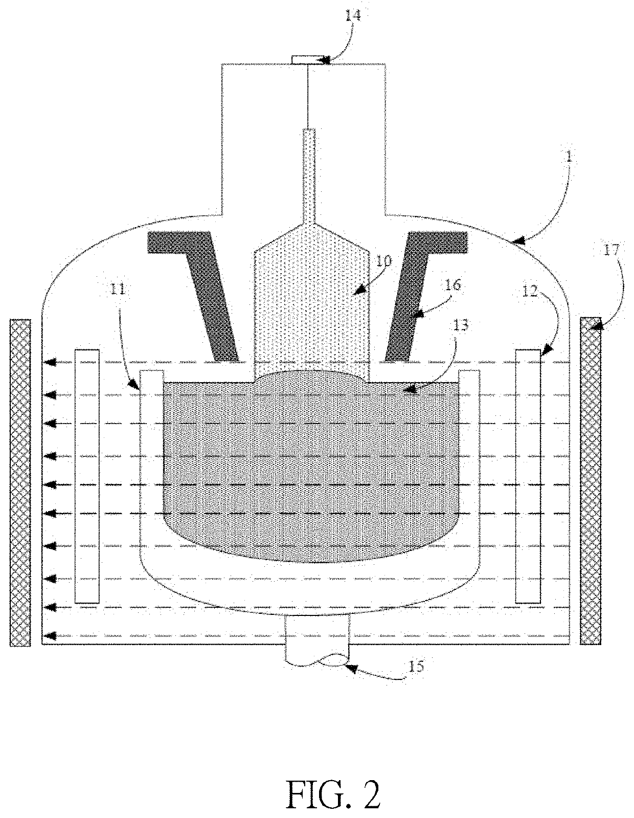
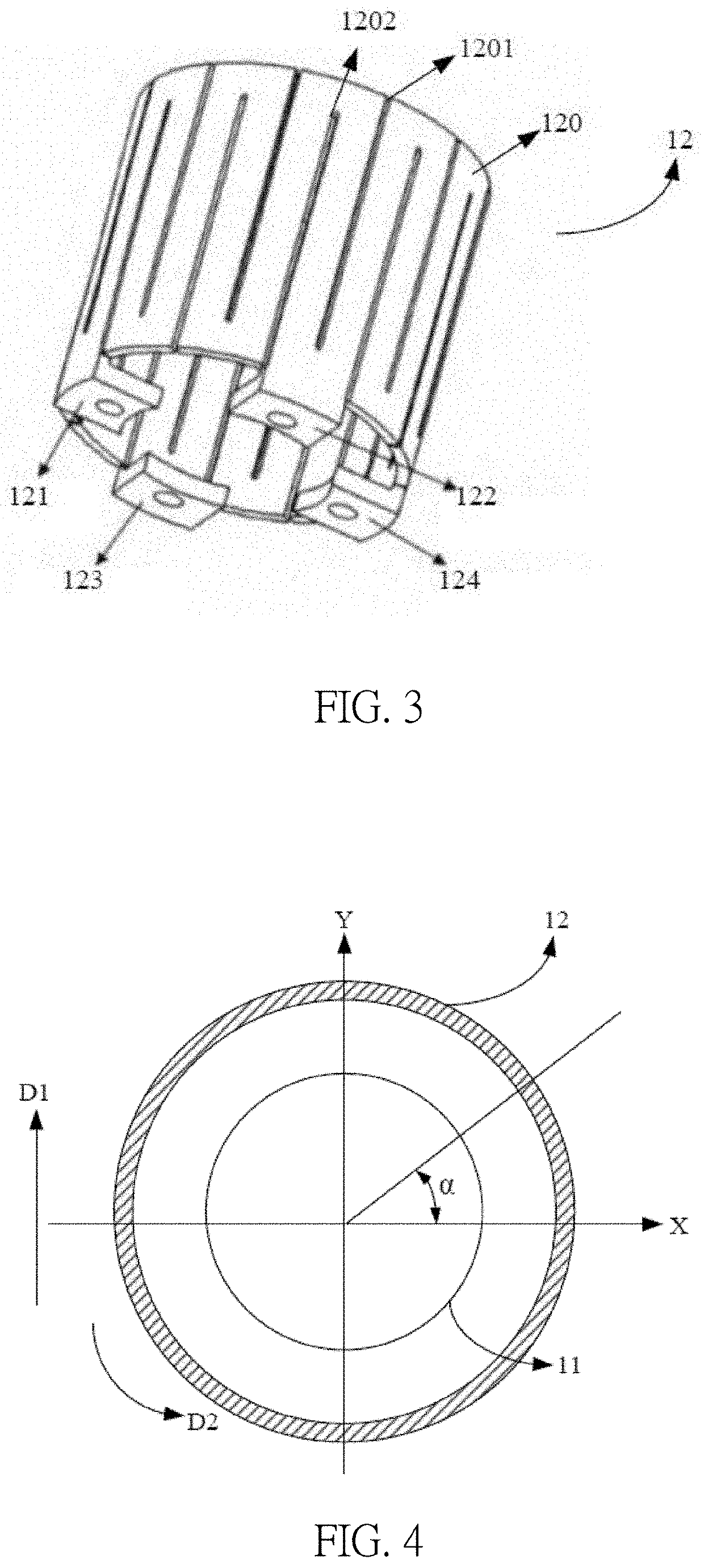
The invention provides a semiconductor crystal growth device. It comprises: a furnace body; a crucible arranged inside the furnace body for containing a silicon melt; a heater having a graphite cylinder arranged around the crucible for heating the silicon melt; a pulling device arranged on the top of the furnace body for pulling out the silicon crystal ingot from the silicon melt; and a magnetic field applying device for applying a horizontal magnetic field to the silicon melt in the crucible; wherein a plurality of grooves are provided on the side wall of the graphite cylinder along the axis direction of the graphite cylinder, and a depth of the grooves in the direction of the magnetic field is smaller than a depth of the grooves perpendicular to the direction of the magnetic field. According to the semiconductor crystal growth device of the present invention, the temperature distribution inside the melt silicon and quality of the semiconductor crystal and the quality of semiconductor crystal growth are improved.

Description

CROSS-REFERENCE TO RELATED APPLICATIONS[0001]This application claims priority to P.R.C. Patent Application No. 201910527728.2 titled “a semiconductor crystal growth apparatus” filed on Jun. 18, 2019, with the State Intellectual Property Office of the People's Republic of China (SIPO).TECHNICAL FIELD[0002]The present invention relates to the field of semiconductor technology, and in particular, to a semiconductor crystal growth device.BACKGROUND[0003]The Czochralski Process (CZ) method is an important method for preparing single crystal silicon for semiconductor and solar energy. The high-purity silicon material placed in the crucible is heated by a thermal field composed of a carbon material to melt it, and then the seed is melted by The crystal is immersed in the melt and undergoes a series of (introduction, shoulder, equal diameter, finishing, cooling) processes to obtain a single crystal rod.[0004]In the growth of semiconductor single crystal silicon or solar single crystal silic...

Claims


Application Information

Patent Timeline
IPC IPC(8): C30B15/14C30B15/00
CPCC30B15/14C30B15/002C30B30/04C30B15/00C30B29/06C30B15/305
Inventor SHEN, WEIMINWANG, GANGDENG, XIANLIANGHUANG, HANYITAN, WEE TECK
Owner ZING SEMICON CORP
Learn More