

Photodiode with antireflective and high conductive metal-semiconductor structure, method for manufacturing the same, and solar cell comprising the same
- Summary
- Abstract
- Description
- Claims
- Application Information
AI Technical Summary
Benefits of technology
Problems solved by technology
Method used
Image

Examples
first embodiment
[0086]FIGS. 8 and 9 illustrate a structure of a schottky photodiode structure using a metal-semiconductor structure with a low reflective and high conductive surface according to the present disclosure and a manufacturing method thereof.
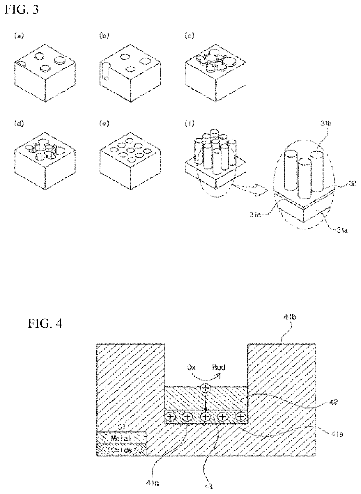
[0087]A schottky photodiode using a metal-semiconductor structure with a low reflective and high conductive surface according to a first embodiment of the present disclosure includes an antireflection semiconductor substrate 81 having an electrode formation area which is selectively etched and a metal catalyst layer 82.
[0088]As seen from a viewpoint of a structure or a morphology, the semiconductor substrate 81 is divided into the electrode formation area 81a which is dug by the etching and the light absorption area 81b which is not etched. Further, the semiconductor substrate further includes a schottky junction area 81c.
[0089]The metal catalyst layer 82a which is buried on the electrode formation area 81a by the etching process entirely form at le...
second embodiment
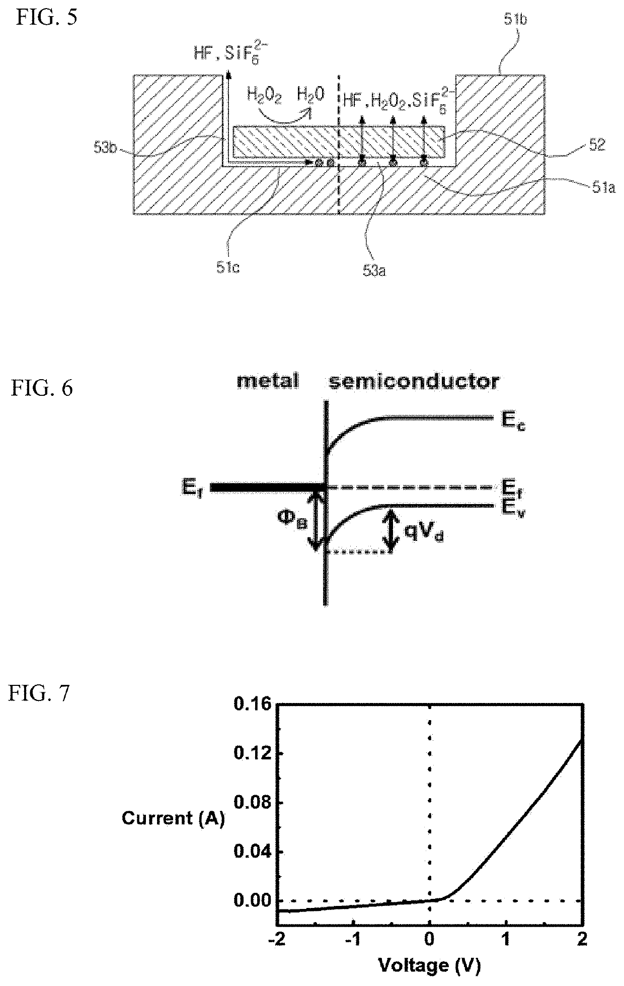
[0105]FIG. 10 is a view illustrating a schottky photodiode structure using a metal-semiconductor structure with a low reflective and high conductive surface according to the present disclosure and a process thereof.
[0106]A schottky photodiode using a metal-semiconductor structure with a low reflective and high conductive surface according to a second embodiment of the present disclosure includes an antireflection semiconductor substrate having an electrode formation area 101a which is selectively etched and a metal catalyst layer 102a formed by placing a metal catalyst used for a metal-assisted chemical etching process employed to form a three-dimensional nanograss structure of the antireflection semiconductor substrate in an etching area of the antireflection semiconductor substrate, that is, a high conductive electrode. An interface between the metal catalyst layer and the electrode formation area is a schottky junction area 101c.
[0107]A manufacturing process of a schottky photod...
PUM
 Abstract
Description
Claims
Application Information