
Method for electrochemically etching a semiconductor structure

a technology of electrochemical etching and semiconductor structure, which is applied in the direction of semiconductor lasers, semiconductor devices, lasers, etc., can solve the problems of increasing the cost of wafer processing, limiting the width of samples that can be porosified, and limiting the distance from an edg

Active Publication Date: 2021-02-25
CAMBRIDGE ENTERPRISE LTD
View PDF0 Cites 2 Cited by
  • Summary
  • Abstract
  • Description
  • Claims
  • Application Information

AI Technical Summary

Benefits of technology

The patent is about a way to improve the process of etching semiconductor materials using electrochemical methods. It suggests using a layer of nanostructures to help create a more favorable environment for the etching process. This arrangement also increases the amount of light that can be extracted from the semiconductor structure.

Problems solved by technology

Horizontal, or lateral, etching from the edge of a sub-surface layer is limited by factors including the diffusion rate of electrolyte into and out of the layer during etching, meaning that there is a limit to the distance from an edge of a layer that can be etched, and therefore that there is a limit to the width of a sample that can be porosified by horizontal etching (if etched from opposite edges).
This additional processing step both increases the cost of wafer processing, and limits the maximum dimension of the resulting porosified structure.
Dividing semiconductor structures into small mesas by dry-etching trenches may also make the resulting porosified structure unsuitable for use in fabrication of certain semiconductor devices.
This technique may therefore limit the viability of horizontal etching methods, and their resulting structures, for practical optoelectronic devices on a large scale.
Where the layer to be etched is not provided as an exposed surface layer, Sandia's PEC technique has therefore been found to result in damage to the surface layer, similarly to the prior art techniques described above.
This etching of the GaN cap surface layer is sometimes described as “vertical etching” in disclosures of Sandia's PEC technique, and is stated to be undesirable but unavoidable, as it damages the surface layer and exposes the layer underneath.

Method used


Image

  • Method for electrochemically etching a semiconductor structure
  • Method for electrochemically etching a semiconductor structure
  • Method for electrochemically etching a semiconductor structure

Examples


Embodiment Construction

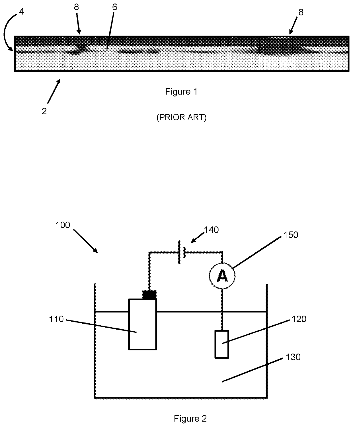
[0267]FIG. 1 shows a scanning TEM micrograph taken from Wang et al (slides), Sandia National Laboratories, showing an etched sample 2. The sample 2 comprises an InGaN quantum well 4 formed as a layer beneath a GaN “cap” layer 6. The sample 2 has been etched using Sandia's “quantum-size-controlled-photoelectrochemical (QSC-PEC)” etching technique. As can be clearly seen in the Figure, the QSC-PEC etching process has damaged the GaN cap layer, creating holes 8 through the entire thickness of the cap layer, so that the etched quantum well layer 4 is exposed. This seems to be the result of undesirable “vertical” etching discussed in publications relating to Sandia's technique.

[0268]The damage Sandia's QSC-PEC technique causes to the GaN cap layer is highly undesirable, as etched quantum structures may be relatively unstable in air. Having the etched layer exposed to the outside environment through holes in the cap layer may therefore cause the etched layer to deteriorate. A further disa...


PUM


Abstract

A method for etching a semiconductor structure (110) is provided, the semiconductor structure comprising a sub-surface quantum structure (30) of a first III-V semiconductor material,beneath a surface layer (31) of a second III-V semiconductor material having a charge carrier density of less than 5×1017 cm3. The sub-surface quantum structure may comprise, for example, a quantum well, or a quantum wire, or a quantum dot. The method comprises the steps of exposing the surface layer to an electrolyte (130), and applying a potential difference between the first III-V semiconductor material and the electrolyte, to electrochemically etch the sub-surface quantum structure (30) to form a plurality of nanostructures, while the surface layer (31) is not etched. A semiconductor structure, uses thereof, and devices incorporating such semiconductor structures are further provided.

Description

[0001]The invention relates to a method for etching a semiconductor material, in particular a III-V semiconductor material, a semiconductor structure, use of a semiconductor structure, and a device incorporating or mounted on a semiconductor structure. In particular, the invention relates to a method of forming quantum dots in a semiconductor structure comprising a sub-surface quantum well, and to semiconductor structures and devices incorporating such semiconductor structures.BACKGROUND[0002]“III-V” semiconductors include binary, ternary and quaternary alloys of Group III elements, such as Ga, Al and In, with Group V elements, such as N, P, As and Sb), and are of great interest for a number of applications, including optoelectronics.[0003]Of particular interest is the class of semiconductor materials known as “Ill-nitride” materials, which includes gallium nitride (GaN), indium nitride (InN) and aluminium nitride (AlN), along with their ternary and quaternary alloys. III-nitride ma...

Claims


Application Information

Patent Timeline
IPC IPC(8): H01L33/00H01L33/02H01L33/06H01L33/10H01L33/32
CPCH01L33/007H01L33/025H01L33/325H01L33/105H01L33/06H01L21/30635H01L33/18H01L33/32H01S5/18316H01S5/3412H01S5/34333
Inventor OLIVER, RACHEL A.ZHU, TONGTONGLIU, YINGJUNGRIFFIN, PETER
Owner CAMBRIDGE ENTERPRISE LTD
Learn More