Chip package structure using silicon interposer as interconnection bridge

a technology of silicon interposer and package structure, applied in the direction of electrical apparatus, semiconductor devices, semiconductor/solid-state device details, etc., can solve the problems of snr degeneration, power consumption performance, and high cost of inter-chip connection, so as to improve signal/consumption performance and facilitate multi-die integration or system in the package. , the effect of improving the signal/consumption performan

Active Publication Date: 2021-03-11
POWERTECH TECHNOLOGY
View PDF0 Cites 20 Cited by
  • Summary
  • Abstract
  • Description
  • Claims
  • Application Information

AI Technical Summary

Benefits of technology

[0015]The chip package structure according to the embodiment of the invention lifts multi-dies allows easier multi-die integration or system in package (SiP) and the shortest connection route also improves the signal / consumption performance.

Problems solved by technology

As for the horizontal placement integration, conventional interconnection between chips is realized by the bottom substrate and redistribution layers (RDL), which have limitations on width / pitch ratio due to the manufacturing capability, thereby setting up the barrier to integration of multi-die structure.
Inter-chip connection hence becomes costly and less efficient, for longer routes or more RDLs are needed.
It is obvious that longer routes and / or more RDLs mean degeneration of SNR and performance of power consumption.

Method used


Image

  • Chip package structure using silicon interposer as interconnection bridge
  • Chip package structure using silicon interposer as interconnection bridge
  • Chip package structure using silicon interposer as interconnection bridge

Examples


first embodiment

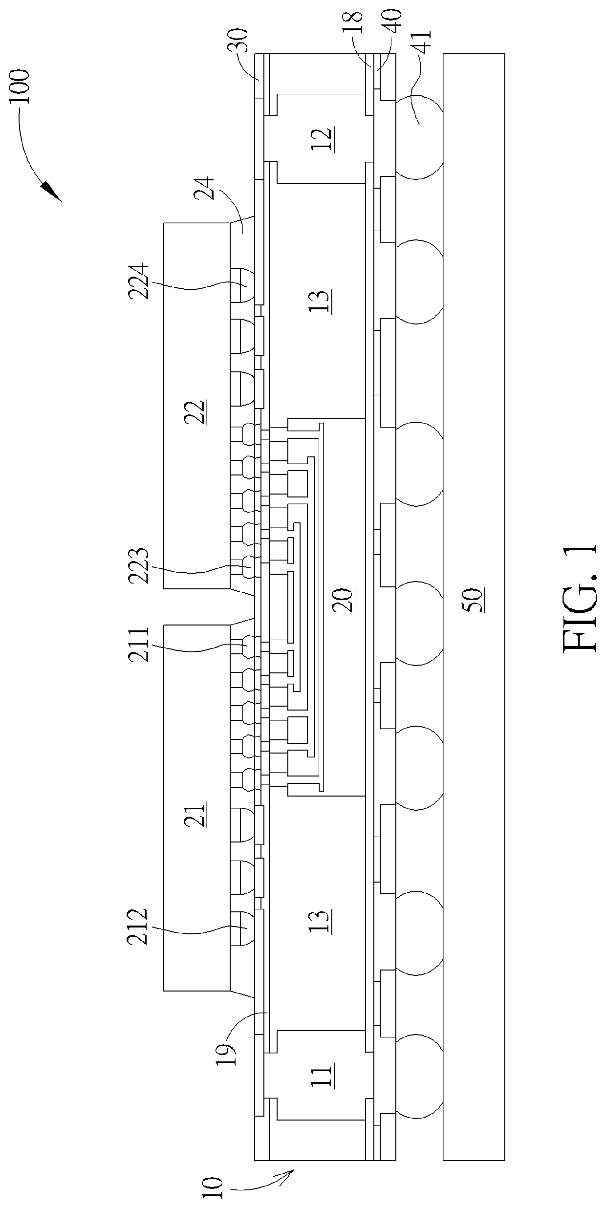
[0023]The interconnection bridge 20 made by advanced procedure is used for interconnection between the first semiconductor die 21 and the second semiconductor die 22. In the first embodiment, silicon interposer with minimum line width / line pitch ratio no greater than 1 / 1 micrometer can be used as the interconnection bridge 20, which is disposed partially in the molding layer 13 and is pre-made by silicon procedure before molding. The interconnection bridge 20 is disposed correspondingly under the plurality of first contacts 211 of the first semiconductor die 21 and the plurality of third contacts 223 of the second semiconductor die 22 in such a way that the plurality of fine-pitched first contacts 211 forms inter-chip connection with the plurality of fine-pitched third contacts 223 through the interconnection bridge 20 following the shortest route. As described earlier, the interconnection bridge 20 using silicon interposer provides minimum line width / line pitch ratio smaller than 1...

fourth embodiment

[0028]Please refer to FIG. 4. The chip package structure 400 in a fourth embodiment in FIG. 4 has substantially the same structure as the aforementioned chip package structures 100, 200, 300, in which same component is designated with the same number. A protective molding layer 60 can be further disposed on the top surface 19 of the fan-out package 10 and covers the first semiconductor die 21 and the second semiconductor die 22 for providing protection for the dies.

[0029]The chip package structure according to the embodiment of the invention lifts multi-dies above the fan-out molding package where at least two dies from the multi-dies are hybrid bump design structure which has both fine pitch and wide pitch design. The premade Si interposer is used as interconnection bridge embedded under the multi-die space for fine pitch high I / O interconnection between dies. The first RDL and the second RDL are further disposed on the top side and the bottom side of the fan-out molding package, f...


PUM


Abstract

A chip package structure using silicon interposer as interconnection bridge lifts multi-dies above the fan-out molding package embedded with premade Si interposer interconnection bridge under the multi-die space. The interconnection bridge connects the multi-dies through fine pitch high I/O interconnection. A first RDL and a second RDL are further disposed on top side and bottom side of the fan-out molding package, further providing connection for the multi-dies to a substrate via the connection routing inside the fan-out molding package.

Description

BACKGROUND OF THE INVENTION1. Field of the Invention[0001]The invention relates to a package structure, and more particularly, to a chip package structure using silicon interposer as interconnection bridge.2. Description of the Prior Art[0002]High level chips have been in increasing demand for product requirements like small size, high I / O count, high thermo performance, and low noise. Back-end processes such as packaging also follow the direction towards reducing the overall package size or integrating more functions in the same chip area and increase the I / O count. It is certainly a trendy development of IC to integrate two or more chips in one package known as multi-die packaging.[0003]Modern technology of multi-die packaging packages two or more than two chips in one chip package by integration (horizontal placement) and / or stacking. As for the horizontal placement integration, conventional interconnection between chips is realized by the bottom substrate and redistribution laye...

Claims


Application Information

Patent Timeline
Patent Type & Authority Applications(United States)
IPC IPC(8): H01L23/538H01L23/498H01L23/31H01L23/00
CPCH01L23/5385H01L23/49872H01L23/3114H01L2224/45147H01L24/45H01L2224/02379H01L24/05H01L25/0655H01L25/50H01L2924/15311H01L2924/15192H01L2224/73204H01L2224/1403H01L2224/16225H01L2224/32225H01L24/16H01L24/32H01L24/73H01L24/14H01L2924/00014H01L23/49816H01L2224/29099H01L2224/13099H01L2924/00
Inventor TSAI, PEI-CHUNHSU, HUNG-HSINCHANG CHIEN, SHANG-YULIN, NAN-CHUN
Owner POWERTECH TECHNOLOGY
Why Eureka
Try Eureka