Silicon nanotube, negative-capacitance transistor with ferroelectric layer and method of making

a technology of ferroelectric layer and negative capacitance, which is applied in the direction of nanotechnology, nanoinformatics, electric devices, etc., can solve the problems of inability to achieve the energy efficiency needed, intimidation of the pace of revolution in the approaching years, and soon unmanageable power consumption

Inactive Publication Date: 2021-03-18
KING ABDULLAH UNIV OF SCI & TECH
View PDF0 Cites 4 Cited by
  • Summary
  • Abstract
  • Description
  • Claims
  • Application Information

AI Technical Summary

Benefits of technology

This patent is about electronic devices that feature a nanotube structure. This structure is formed by creating a trench in the body of the device and filling it with a nanotube material. The nanotube structure is then separated from the body by a layer of material called a gate dielectric layer and a ferroelectric layer. In some embodiments, the nanotube structure includes a source region, a channel region, and a drain region. The invention allows for the formation of electronic devices with improved performance and function.

Problems solved by technology

With the exponential growth of information infrastructure, the power consumption will soon reach unmanageable levels.
Therefore, power dissipation and management concerns in the information infrastructure will intimidate the pace of the revolutions in the approaching years.
However, the downscaling of the devices was not able to achieve the energy efficiency needed, and the drain voltage Vdd applied to the drain of a transistor was not able to scale below 1 V for almost 15 years.
In addition, the clock frequency remained at about 3 GHz after 2005 due to the unmanageable power density beyond 100 W / cm2.
Thus, modern electronic devices and evolving IoT technologies require extremely low-power, large-scale-integration and low-cost systems.
Thus, ultralow power consumption (e.g., sub 1 μW) is needed for data sensing / processing / communication in this field.
However, this approach results in a lower Ion and higher circuit delay while the leakage current keeps flowing.

Method used


Image

  • Silicon nanotube, negative-capacitance transistor with ferroelectric layer and method of making
  • Silicon nanotube, negative-capacitance transistor with ferroelectric layer and method of making
  • Silicon nanotube, negative-capacitance transistor with ferroelectric layer and method of making

Examples


Embodiment Construction

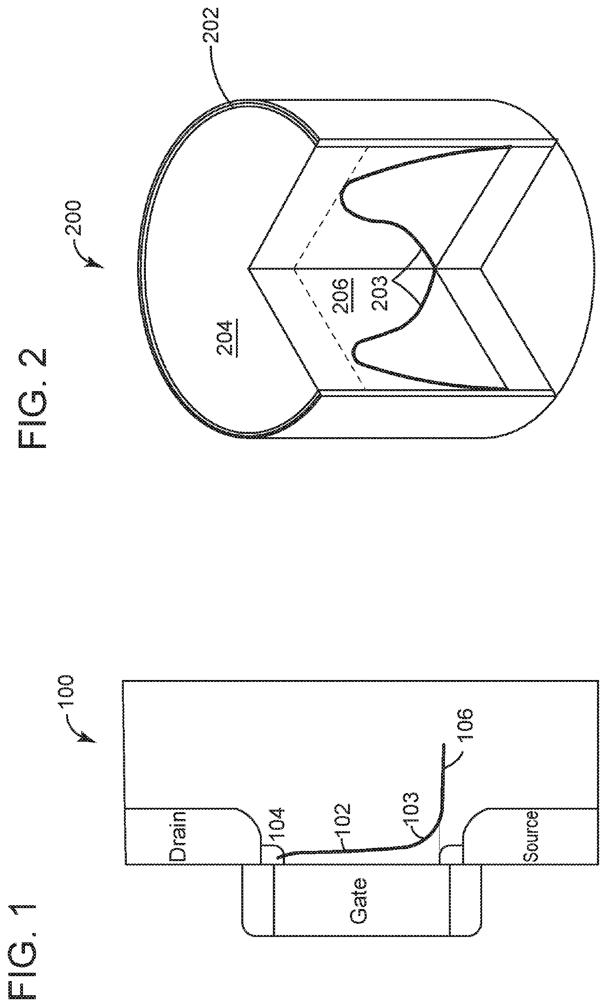
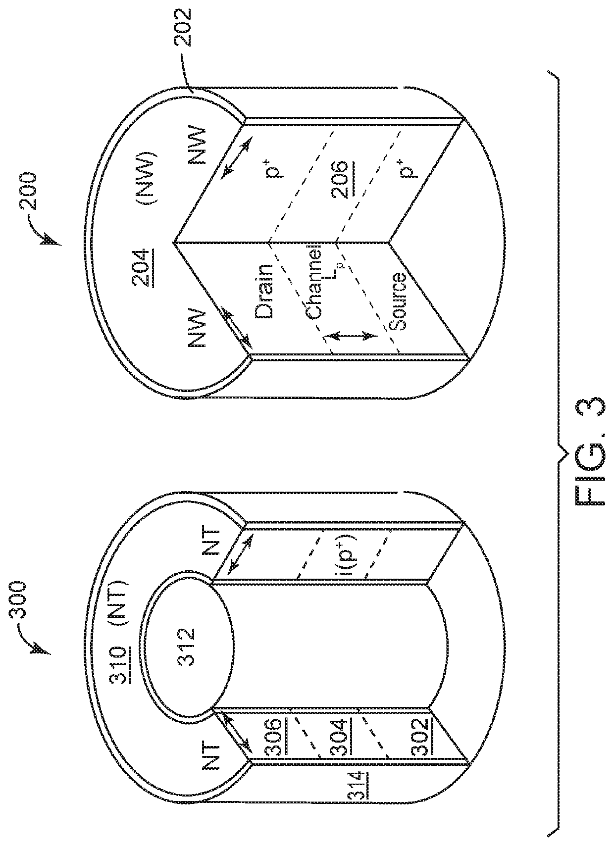
[0020]The following description of the embodiments refers to the accompanying drawings. The same reference numbers in different drawings identify the same or similar elements. The following detailed description does not limit the invention. Instead, the scope of the invention is defined by the appended claims. The following embodiments are discussed, for simplicity, with regard to a nanotube, negative-capacitance (NC), field effect transistor (FET) with ferroelectric layers. However, the embodiments discussed herein are not limited to this transistor, but may be applied to other transistors.

[0021]Reference throughout the specification to “one embodiment” or “an embodiment” means that a particular feature, structure or characteristic described in connection with an embodiment is included in at least one embodiment of the subject matter disclosed. Thus, the appearance of the phrases “in one embodiment” or “in an embodiment” in various places throughout the specification is not necessa...


PUM


Abstract

There is a an electronic device that includes a substrate; a body including plural layers, the body being formed on top of the substrate; a nanotube trench formed vertically in the body and extending to the substrate; and a nanotube structure formed in the nanotube trench. The nanotube structure is mechanically separated from the body by a gate dielectric layer and a ferroelectric layer.

Description

CROSS-REFERENCE TO RELATED APPLICATIONS[0001]This application claims priority to U.S. Provisional Patent Application No. 62 / 610,375, filed on Dec. 26, 2017, entitled “SI NANOTUBE NEGATIVE-CAPACITANCE FIELD EFFECT TRANSISTOR FOR LOW-POWER NANOSCALE DEVICES,” and U.S. Provisional Patent Application No. 62 / 674,693, filed on May 22, 2018, entitled “SILICON NANOTUBE, NEGATIVE-CAPACITANCE TRANSISTOR WITH FERROELECTRIC LAYER AND METHOD OF MAKING,” the disclosures of which are incorporated herein by reference in their entirety.BACKGROUNDTechnical Field[0002]Embodiments of the subject matter disclosed herein generally relate to a silicon nanotube negative-capacitance transistor, and more specifically, to a silicon nanotube negative-capacitance field effect transistor with ferroelectric layers that uses low-power.Discussion of the Background[0003]Currently, all the online activities in the United States are driven by 12 million servers which are distributed in 3 million data centers, and thei...

Claims


Application Information

Patent Timeline
IPC IPC(8): H01L29/06H01L29/66H01L29/775H01L29/78
CPCH01L29/0676H01L29/66439H01L29/78391H01L29/7827H01L29/7831H01L29/775B82Y10/00H01L29/42356
Inventor HUSSAIN, MUHAMMAD MUSTAFAEL-ATAB, NAZEK MOHAMAD
Owner KING ABDULLAH UNIV OF SCI & TECH
Why Eureka
Try Eureka