Dual-gated memtransistor crossbar array, fabricating methods and applications of same

a dual-gated, cross-bar array technology, applied in the field of semiconductors, can solve the problems of limited scaling to the same level as conventional dynamic random access memory (dram), synaptic transistors do not offer control over learning rate, gate terminals in synaptic transistors are not available for additional tunability over current-voltage characteristics, etc., to achieve high-scale effects

Pending Publication Date: 2021-04-01
NORTHWESTERN UNIV
View PDF9 Cites 16 Cited by
  • Summary
  • Abstract
  • Description
  • Claims
  • Application Information

AI Technical Summary

Benefits of technology

[0008]One of the objectives of this invention is to provide dual-gated MoS2 memtransistors enabling artificial synapses with tunable learning rates where the two gates act as modulatory terminals that mimic biological systems. In crossbar arrays, these dual-gated memtransistors also overcome the sneak current issue that plagues conventional memristors. The non-volatile resistance states and read currents are controlled by distinct metal lines in the crossbar array, providing a highly scalable paradigm for neuromorphic circuits.
[0024]In one embodiment, the memtransistor is configured such that both long-term potentiation (LTP) and long-term depression (LTD) are operably modulated as a function of the gate bias during writing, while the output current during reading is operably controlled as a function of the gate bias during reading without affecting the intrinsic state of the memtransistor.
[0052]In one embodiment, the crossbar array is configured such that each memtransistor is writable and readable independently, thereby minimizing sneak current in the crossbar array.
[0053]In one embodiment, the crossbar array is configured such that application of a predetermined bottom gate voltage suppresses read currents without changing non-volatile memristive resistance states of the memtransistors in the crossbar array, thereby enabling isolation of the non-volatile memristive resistance states and read currents without additional elements at each node for crossbar operation in the crossbar array.
[0055]In one embodiment, a linear and symmetric learning behavior that produces efficient training of an artificial neural network (ANN) is achievable by the gate tunability.

Problems solved by technology

While a significant advantage of memristors is their scalability via crossbar arrays, this same architecture also imposes two major challenges.
Second, reliable access to individual nodes in a crossbar architecture requires a non-linear (i.e., diode) or active (i.e., transistor) component at each node, limiting scaling to the same level as conventional dynamic random access memory (DRAM).
However, synaptic transistors do not offer control over learning rate and require an additional element at each node for individual device access in a crossbar architecture since their non-volatile resistance states are written by a gate bias and read by a drain current.
Thus, despite being a three-terminal device, the gate terminal in a synaptic transistor is not available for additional tunability over the current-voltage characteristics.
Therefore, a heretofore unaddressed need exists in the art to address the aforementioned deficiencies and inadequacies.

Method used


Image

  • Dual-gated memtransistor crossbar array, fabricating methods and applications of same
  • Dual-gated memtransistor crossbar array, fabricating methods and applications of same
  • Dual-gated memtransistor crossbar array, fabricating methods and applications of same

Examples


Embodiment Construction

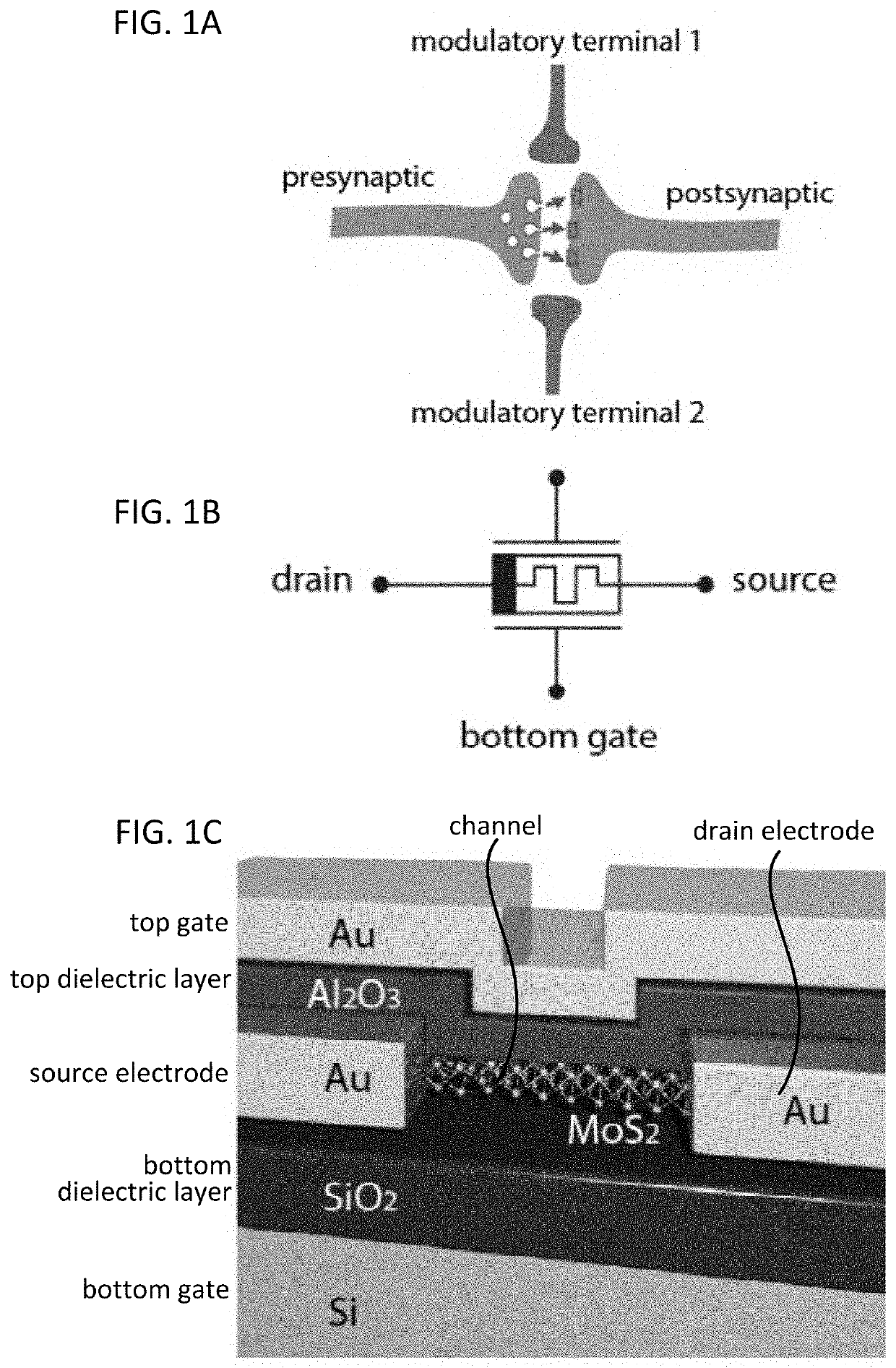
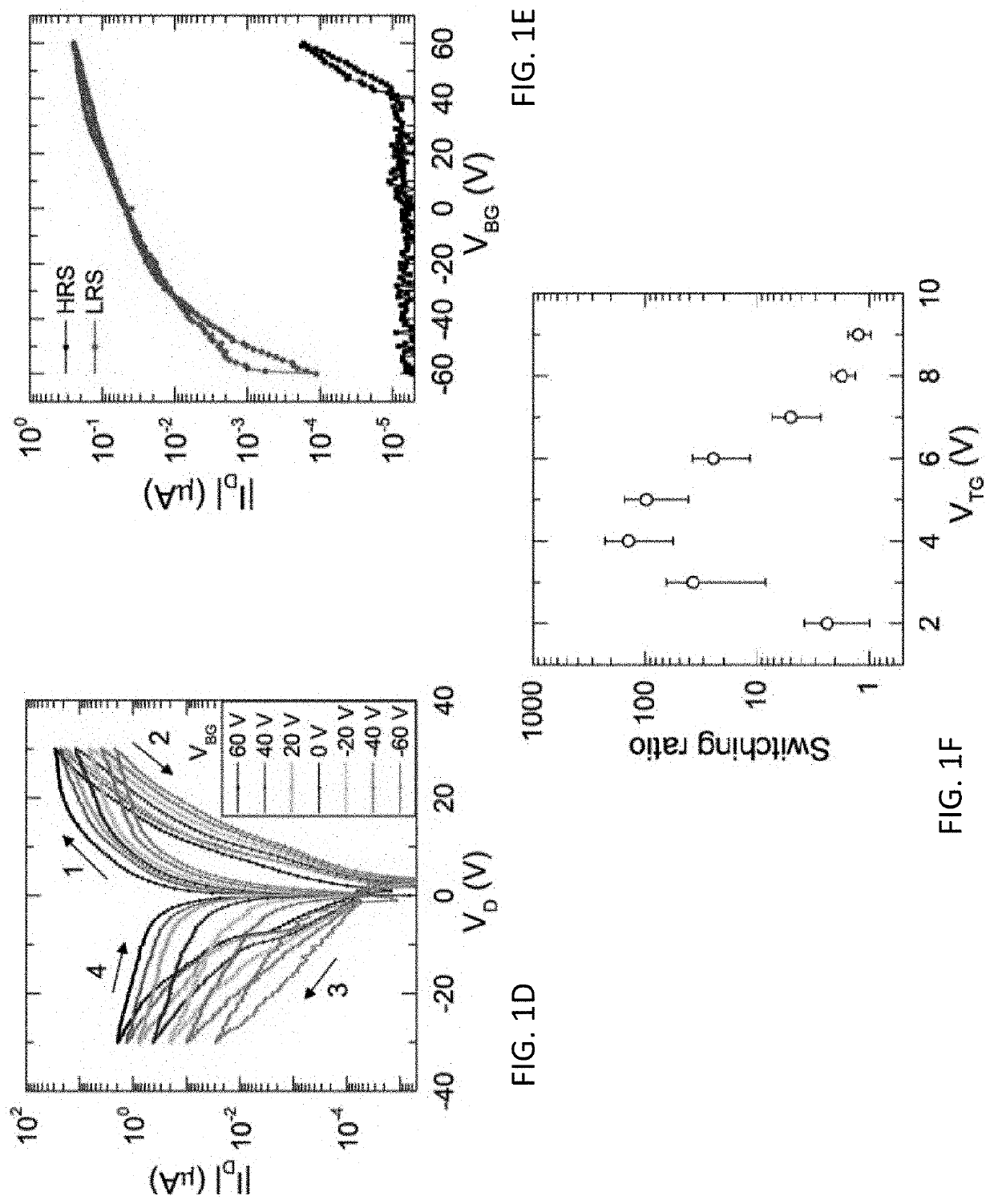
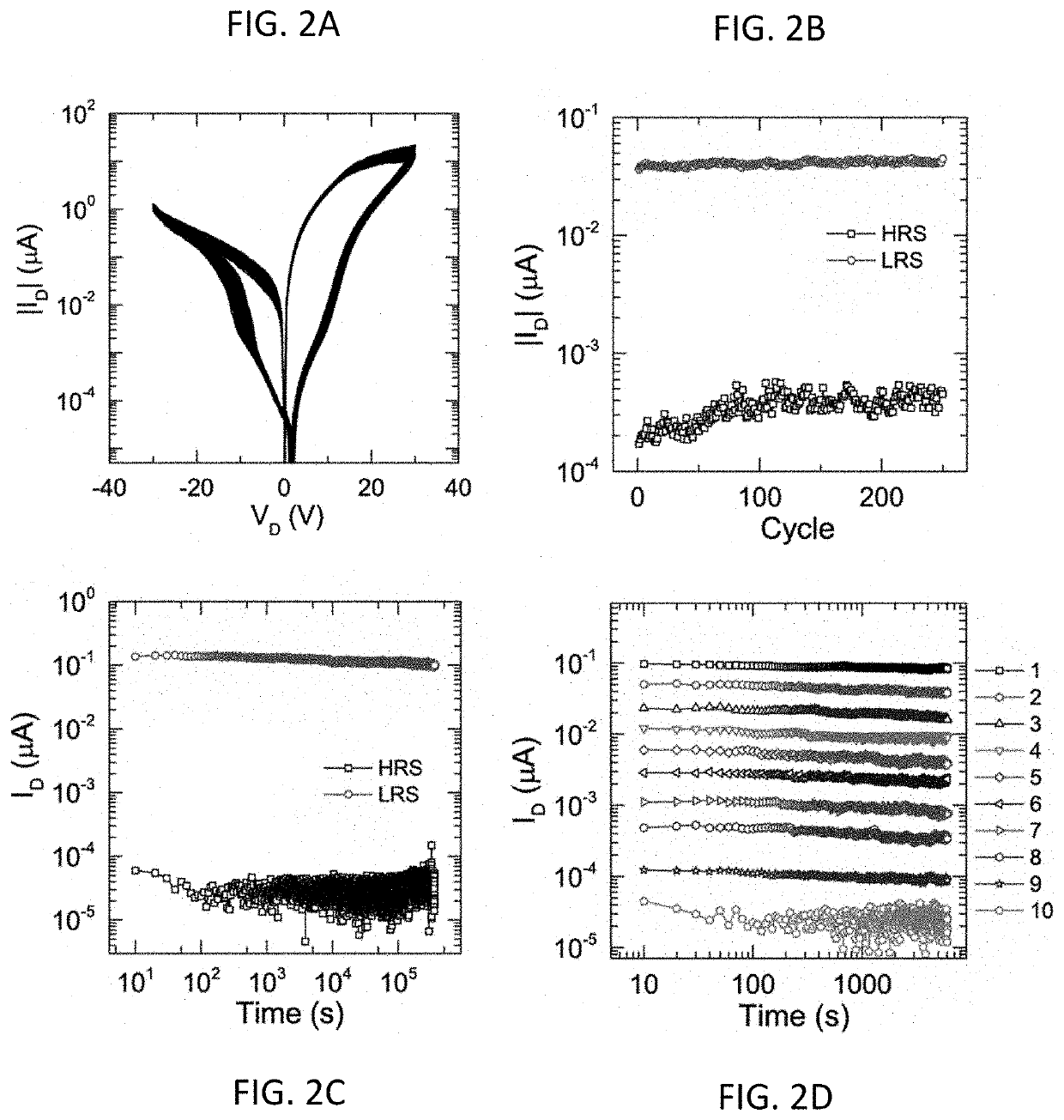
lass="d_n">[0093]The invention will now be described more fully hereinafter with reference to the accompanying drawings, in which exemplary embodiments of the invention are shown. This invention may, however, be embodied in many different forms and should not be construed as limited to the embodiments set forth herein. Rather, these embodiments are provided so that this specification will be thorough and complete, and will fully convey the scope of the invention to those skilled in the art. Like reference numerals refer to like elements throughout.

[0094]The terms used in this specification generally have their ordinary meanings in the art, within the context of the invention, and in the specific context where each term is used. Certain terms that are used to describe the invention are discussed below, or elsewhere in the specification, to provide additional guidance to the practitioner regarding the description of the invention. For convenience, certain terms may be highlighted, for...


PUM

PropertyMeasurementUnit
spot sizeaaaaaaaaaa
grain sizesaaaaaaaaaa
currentaaaaaaaaaa

Abstract

A memtransistor includes a top gate electrode and a bottom gate electrode; a polycrystalline monolayer film formed of an atomically thin material disposed between the top gate electrode and the bottom gate electrode; and source and drain electrodes spatial-apart formed on the polycrystalline monolayer film to define a channel in the polycrystalline monolayer film between the source and drain electrodes. The top gate electrode and the bottom gate electrode are capacitively coupled with the channel.

Description

CROSS-REFERENCE TO RELATED PATENT APPLICATIONS[0001]This application claims priority to and the benefit of U.S. Provisional Application Ser. No. 62 / 908,841, filed Oct. 1, 2019, which is incorporated herein in its entirety by reference.STATEMENT AS TO RIGHTS UNDER FEDERALLY-SPONSORED RESEARCH[0002]This invention was made with government support under 70NANB14H012 awarded by the National Institute of Standards and Technology, and DMR-1720139 awarded by the National Science Foundation. The government has certain rights in the invention.FIELD OF THE INVENTION[0003]The present invention relates generally to semiconductors, and more particularly to a dual-gated memtransistor crossbar array, fabricating methods and applications of the same.BACKGROUND OF THE INVENTION[0004]The background description provided herein is for the purpose of generally presenting the context of the invention. The subject matter discussed in the background of the invention section should not be assumed to be prior...

Claims


Application Information

Patent Timeline
Patent Type & Authority Applications(United States)
IPC IPC(8): H01L29/68H01L27/12H01L29/24H01L29/66H01L29/739G06N3/04G06N3/08
CPCH01L29/685H01L27/1225H01L29/24H01L29/66969H01L29/0665H01L27/127G06N3/04G06N3/08H01L29/7394H01L29/778H01L29/78696H01L29/78681H01L29/7831H01L29/7839H01L29/04G11C11/54G11C13/0033G11C13/004G11C13/0069G11C13/003G11C2213/82G11C2213/53G11C13/0002G11C13/0007B82Y10/00G06N3/049G06N3/065H10B99/00H01L29/1033H01L29/4908
Inventor HERSAM, MARK C.SANGWAN, VINOD K.LEE, HONG-SUB
Owner NORTHWESTERN UNIV
Why Eureka
Try Eureka