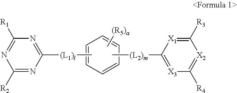
Compound and organic light-emitting device including the same
- Summary
- Abstract
- Description
- Claims
- Application Information
AI Technical Summary
Benefits of technology
Problems solved by technology
Method used
Image
Examples
examples — synthesis example
Examples—Synthesis Example: Synthesis of Compounds
[0346]Polycyclic compounds according to some exemplary embodiments may be synthesized by using, for example, the following methods. However, other synthesis methods for the polycyclic compounds may be used.
[0347]Synthesis of Compound 2
[0348]Polycyclic compound 2 according to some exemplary embodiments may be synthesized according to, for example, the following Reaction Scheme 1.
[0349]Synthesis of Intermediate 1-3
[0350]2,4-dichloro-6-phenyl-1,3,5-triazine (CAS:1700-02-3) and (3-(triphenylsilyl)phenyl)boronic acid (CAS:1253912-58-1) were reacted in the presence of Pd catalyst to obtain Intermediate 1-3. Intermediate 1-3 was confirmed by liquid chromatograpy-mass spectroscopy (LC-MS).
[0351]C33H24ClN3Si M+1: 526.36
[0352]Synthesis of Compound 2
[0353]0.3 g of 1,3-phenylboronic acid, 2.19 g of Intermediate 1-3, 0.08 g of tetrakis(triphenylphosphine)palladium, and 0.62 g of potassium carbonate were added to a reaction container and dissolved...
example 1
[0393]As an anode, a 15 Ω / cm2 (1,200 Å) ITO glass substrate available from Corning, Inc. of Corning, N.Y. (hereinafter “Corning”) was cut to a size of 50 mm×50 mm×0.7 mm, sonicated with isopropyl alcohol and pure water each for 5 minutes, and then cleaned by exposure to ultraviolet rays and ozone for 30 minutes. The ITO glass substrate was provided to a vacuum deposition apparatus.
[0394]A known compound NPD was vacuum-deposited on the ITO glass substrate to form a hole injection layer having a thickness of 300 Å, and then (4-chloro-2-methylphenoxy)acetic acid (mCP) was vacuum-deposited on the hole injection layer to form a hole transport layer having a thickness of 200 Å.
[0395]Compound 2 and FD1 were co-deposited on the hole transport layer at a weight ratio of 92:8 to form an emission layer having a thickness of 250 Å. Then, as a compound for an electron transport layer, TAZ was deposited thereon to form an electron transport layer having a thickness of 200 Å.
[0396]LiF, which is a ...
example 2
[0397]An organic light-emitting device was manufactured in the same manner as in Example 1, except that Compound 7 was used instead of Compound 2 in forming the emission layer.
PUM
 Abstract
Description
Claims
Application Information
 - R&D
- Intellectual Property
- Life Sciences
- Materials
- Tech Scout
- Unparalleled Data Quality
- Higher Quality Content
- 60% Fewer Hallucinations
Browse by: Latest US Patents, China's latest patents, Technical Efficacy Thesaurus, Application Domain, Technology Topic, Popular Technical Reports.
© 2025 PatSnap. All rights reserved.Legal|Privacy policy|Modern Slavery Act Transparency Statement|Sitemap|About US| Contact US: help@patsnap.com


