High-resolution 3D radar wave imaging device

a high-resolution, radar wave technology, applied in the direction of protective material radiating elements, polarised antenna unit combinations, instruments, etc., can solve the problems of insufficient azimuthal and elevational resolution of current radar devices, ambiguity in angular reconstruction, etc., to improve the characterization of objects in the scene, reduce or even eliminate the effect of almost eliminating

Active Publication Date: 2021-05-06
IEE INT ELECTRONICS & ENG SA
View PDF0 Cites 8 Cited by
  • Summary
  • Abstract
  • Description
  • Claims
  • Application Information

AI Technical Summary

Benefits of technology

[0024]In this way, the function of beamforming is performed by the imaging radar optics unit without any need for employing a beamforming method. Therefore, the radar wave imaging device is not based on digital beam forming techniques for a phased array that are known in the art, such as Barlett beamformer, Minimum Variance Distortionless Response (CAPON) beamformer or advanced beamforming methods such as MUSIC (MUltiple Signal Classification) and ESPRIT (Estimation of Signal Parameters by Rotation Invariant Techniques). In a suitable embodiment, a large detector array integrated on an integrated circuit can be provided. Using a high-refractive index material radar lens allows utilizing the high resolving power of the radar lens in order to image the scene, yielding a substantial increase in angular resolution compared to conventional small to mid-sized phased arrays.
[0059]Using now the radar receiver members with the imaging system, each antenna member (or pixel) of the radar receiver member having a size Δx (in the same direction as d for the Tx antenna array above) collects electromagnetic radiation from the field of view region associated with it. The angular width of said FOV may be written in a first approximation asΔ⁡(sin⁢⁢Θpix)=n⁢⁢Δ⁢xf,n denoting the refractive index of the high refractive material of the first lens, and f the focal length of the first lens. By ensuring that Δ(sin Θi)≅Δ(sin Θpix), the ambiguities given for any real m>1 in the transmit array can be lifted. Typically the values should be chosen such thatΔ(sin Θpix)<1.2*Δ(sin Θi), preferably 0.5Δ(sin Θi)≤Δ(sin Θpix)≤Δ(sin Θi).Of all possible AoA solutions, Θi, only the real target AoA will result in a substantial signal in the receiver member of which the FOV contains the target's AoA. Thereby subpixel angular resolution on the array consisting of the plurality of receiver members can be achieved without ambiguity.

Problems solved by technology

In automotive radar applications one challenge is to determine the Direction of Arrival (DoA) of incoming radar waves which were transmitted towards and were reflected by targets.
However, a displacement of the antennas by multiple wavelengths leads to ambiguity in angular reconstruction when performed with conventional digital beam forming (DBF) methods.
An angular resolution of current radar devices, both in azimuthal and elevational direction, is not sufficient e.g. for automotive ADAS (Advanced Driver Assistance Systems) requirements, and neither for aerospace applications such as in drones and helicopters.
Using principles like digital beam forming (DBF) or beam steering, an angular resolution can be increased using additional individual antenna members in a large planar antenna array (phased array), however:Size and complexity of a feed structure on a planar antenna substrate (so called front-end printed circuit board (PCB) made, for instance, of a PCB material suitable for the frequencies of radar operation) is a limiting factor for large cost-efficient phased arrays in small devices.The large size of a multi-element phased array, by way of example 100 antenna members in a gate array (also called uncommitted logic array (ULA)) spaced by half a wavelength at a radar carrier frequency of 77 GHz would result in a dimension of about 20 cm, which is prohibitive for integration in passenger cars.Due to a large overall size of the phased array, a required length of feed transmission lines of the individual antenna members will affect and limit the signal-to-noise ratio (SNR) of the radar device.Alternatively, in case that distributed ICs (integrated circuits) are used for radar signal generation and detection that are arranged in close proximity to the individual antennas of the large phased array, the complexity of manufacturing increases substantially, as many individual ICs have to be connected by high-precision processes to the front-end PCB.

Method used


Image

  • High-resolution 3D radar wave imaging device
  • High-resolution 3D radar wave imaging device
  • High-resolution 3D radar wave imaging device

Examples


Embodiment Construction

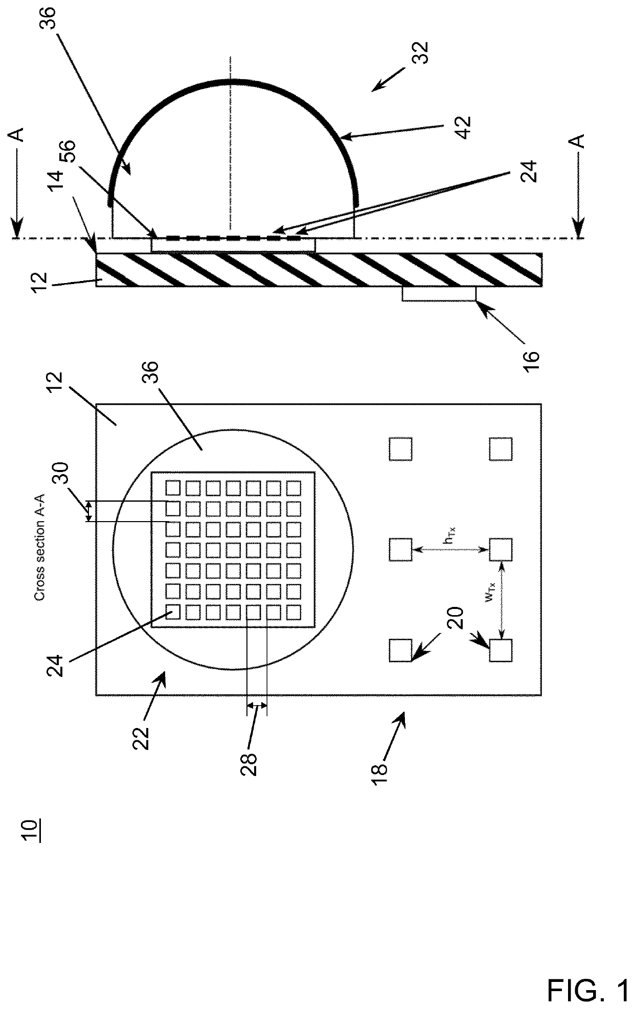
>[0077]FIG. 1 schematically illustrates a possible embodiment of the radar wave imaging device 10 in accordance with the invention. The radar wave imaging device 10 includes a radar transmitter unit 18 and a radar receiving unit 22.

[0078]The radar transmitter unit 18 comprises a plurality of six radar transmit antennas 20 that are regularly arranged as a two by three two-dimensional array on a right side portion of a front surface 14 of a substrate plate 12 and connected to a transmitter circuitry 16. The radar transmit antennas 20 are directed towards a scene in front of the substrate plate 12. The scene may comprise objects, temporarily forming part of the scene, that are to be detected by the radar wave imaging device 10. The radar transmit antennas 20 of the radar transmitter unit 18 are configured for transmitting radar waves towards the scene. It should be noted that the transmitter circuitry 16 may be arranged below the substrate plate 12 as shown in FIG. 1, but it could also...


PUM


Abstract

A radar wave imaging device includes a radar transmitter unit having at least one radar transmit antenna for transmitting radar waves towards a scene and a radar receiving unit including a plurality of radar receiver members that are arranged as a two-dimensional array, for receiving reflected radar waves. The radar receiving unit includes an imaging radar optics unit for imaging at least a portion of a scene onto at least a portion of the two-dimensional array of radar receiver members. The imaging radar optics unit includes at least a first radar lens that is arranged between the radar receiver members and the scene. The radar receiver members are arranged in direct contact to a surface of the first radar lens that is facing away from the scene.

Description

TECHNICAL FIELD[0001]The invention generally relates to a radar wave imaging device, usable for various applications such as people monitoring, building management and security as well as applications on moving platforms such as small unmanned aerial systems and automotive vehicles, and for sensing applications in the domain of Internet of Things.BACKGROUND OF THE INVENTION[0002]It is known in the art of military and avionic technology to employ radar technology. More recently the development of radar sensors has focused on the automotive field, in particular employing radar technology in the millimeter wave range between 75 and 81 GHz, in exterior automotive applications such as automotive ADAS (Advanced Driver Assistance Systems) for providing improved safety by facilitating an optimized reaction of a driver of a vehicle with appropriate warnings or even by automatically taking over control of the vehicle, for instance in collision avoidance systems.[0003]In automotive radar appli...

Claims


Application Information

Patent Timeline
Patent Type & Authority Applications(United States)
IPC IPC(8): H01Q21/06H01Q19/09H01Q21/24H01Q9/04G01S13/32G01S13/42G01S17/89G01S7/03
CPCH01Q21/065H01Q19/09H01Q21/24G01S7/032G01S13/32G01S13/42G01S17/89H01Q9/0457G01S7/481G01S13/89H01Q1/40H01Q1/523H01Q9/0407H01Q13/10H01Q15/02H01Q19/062H01Q1/2283H01Q1/3233H01Q9/045G01S7/027
Inventor SPIELMANN, THIEMOHERSCHBACH, NORBERT
Owner IEE INT ELECTRONICS & ENG SA
Why Eureka
Try Eureka