
Method of forming graphene

a graphene and graphene technology, applied in the field of forming graphene, can solve the problems of difficult to form graphene having uniform flatness and difficult diffusion of carbon sources, and achieve the effect of uniform flatness

Pending Publication Date: 2021-06-03
SAMSUNG ELECTRONICS CO LTD
View PDF3 Cites 1 Cited by
  • Summary
  • Abstract
  • Description
  • Claims
  • Application Information

AI Technical Summary

Benefits of technology

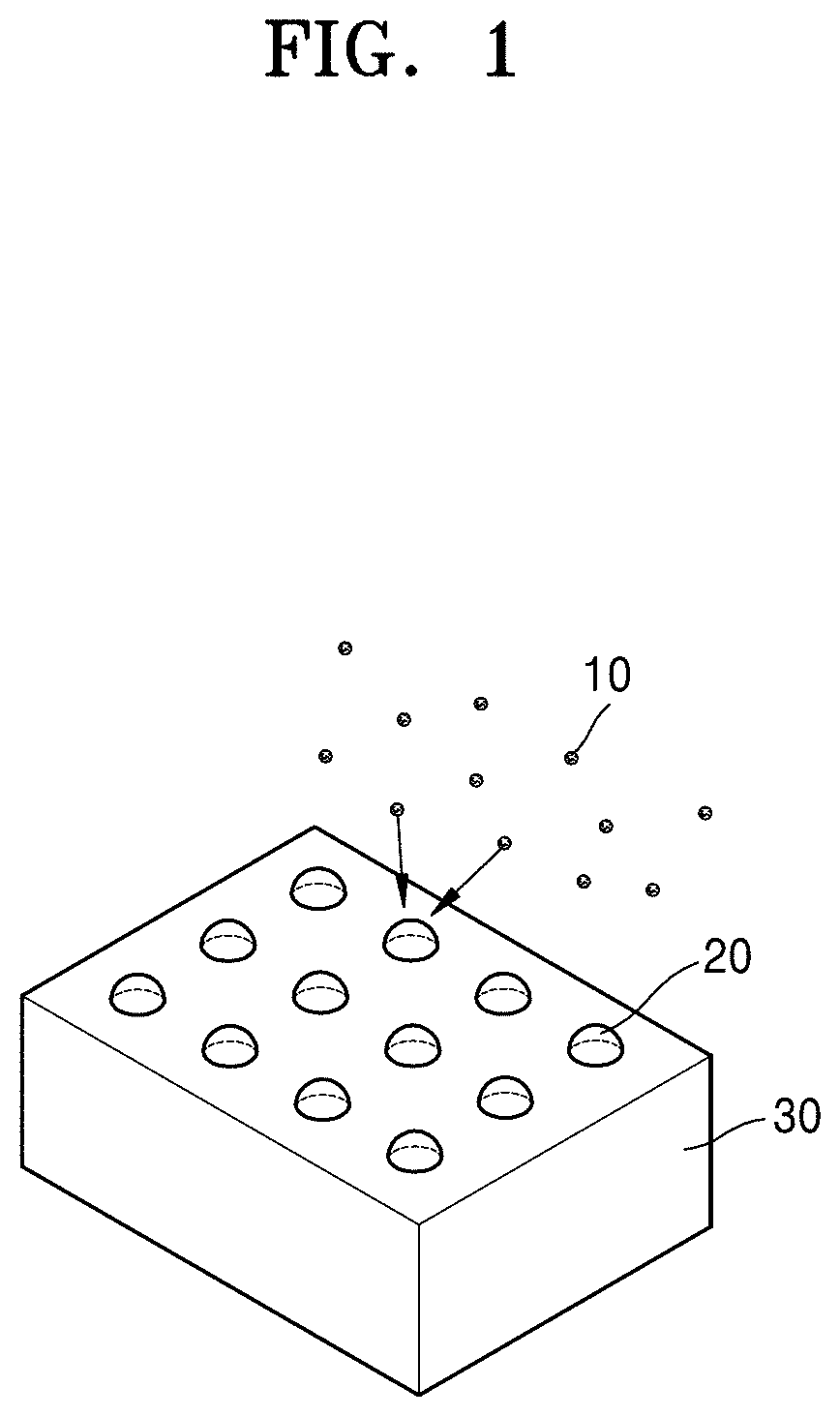
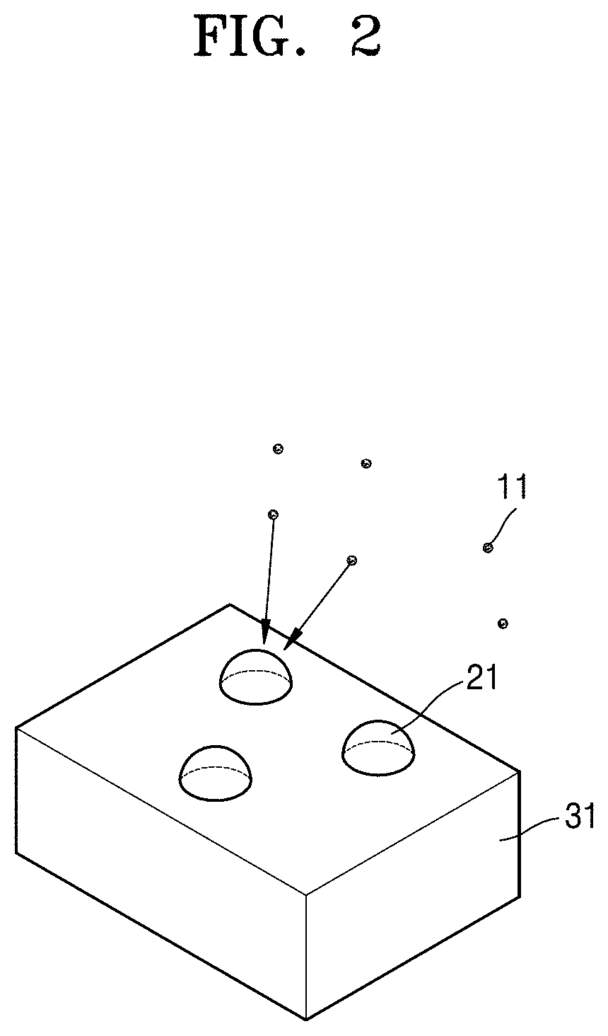
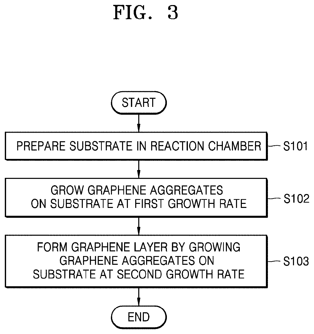
The patent describes a method for forming high-quality graphene layers on a substrate with uniform flatness. The method involves preparing the substrate and then performing two growth processes using a reaction gas containing a carbon source. The first growth process involves growing a plurality of graphene aggregates on the substrate at a high growth rate, while the second growth process involves growing the aggregates at a slower rate. The second growth process results in a graphene layer with a higher coverage of the substrate compared to the first growth process. The method can be performed using a plasma enhanced chemical vapor deposition (PECVD) process at a process temperature of 200° C to 700° C. The substrate can include non-catalyst materials such as silicon, semiconductor compounds, insulating materials, and dopants. The carbon source can be a hydrocarbon in a liquid state at room temperature. The method can also include pretreating the substrate surface before the first growth process. Overall, the method provides a reliable and effective way to form high-quality graphene layers on various substrates.

Problems solved by technology

In order to apply graphene to a semiconductor device, when graphene is directly grown on a non-catalyst substrate in a low-temperature environment, induction of diffusion of a carbon source is not easy due to the low-temperature environment, and thus it may be difficult to form graphene having uniform flatness.

Method used


Image

  • Method of forming graphene
  • Method of forming graphene
  • Method of forming graphene

Examples


Embodiment Construction

[0051]Reference will now be made in detail to embodiments, examples of which are illustrated in the accompanying drawings, wherein like reference numerals refer to like elements throughout. In this regard, the present embodiments may have different forms and should not be construed as being limited to the descriptions set forth herein. Accordingly, the embodiments are merely described below, by referring to the figures, to explain aspects. As used herein, the term “and / or” includes any and all combinations of one or more of the associated listed items. Expressions such as “at least one of,” when preceding a list of elements (e.g., A, B, and C), modify the entire list of elements and do not modify the individual elements of the list. For example, “at least one of A, B, and C,”“at least one of A, B, or C,”“one of A, B, C, or a combination thereof,” and “one of A, B, C, and a combination thereof,” respectively, may be construed as covering any one of the following combinations: A; B; A...


PUM

PropertyMeasurementUnit
pressureaaaaaaaaaa
temperatureaaaaaaaaaa
pressureaaaaaaaaaa

Abstract

A method of forming graphene includes: preparing a substrate in a reaction chamber; performing a first growth process of growing a plurality of graphene aggregates apart from each other on the substrate at a first growth rate by using a reaction gas including a carbon source; and performing a second growth process of forming a graphene layer by growing the plurality of graphene aggregates at a second growth rate slower than the first growth rate by using the reaction gas including the carbon source.

Description

CROSS-REFERENCE TO RELATED APPLICATION[0001]This application claims the benefit of Korean Patent Application No. 10-2019-0159352, filed on Dec. 3, 2019, in the Korean Intellectual Property Office, the disclosure of which is incorporated herein in its entirety by reference.BACKGROUND1. Field[0002]The present disclosure relates to a method of forming graphene, and more particularly, to a method of forming graphene directly on a substrate.2. Description of Related Art[0003]In the semiconductor device field, resistance increases as the width of metal wiring decreases. Graphene is being actively researched in the semiconductor device field and research is being done to develop a new metal barrier material. Graphene is a material that has a hexagonal honeycomb structure in which carbon atoms are connected two-dimensionally, and has a very small thickness at the atomic size. Such graphene has advantages of high electric mobility, excellent thermal characteristics, chemical stability, and a...

Claims


Application Information

Patent Timeline
Patent Type & Authority Applications(United States)
IPC IPC(8): C01B32/186
CPCC01B32/186H01L29/1606H01L21/02274C01B32/182H01L21/324Y10T428/30
Inventor NGUYEN, VAN LUANSHIN, KEUNWOOKSHIN, HYEONJINKIM, CHANGHYUNLEE, CHANGSEOKCHO, YEONCHOO
Owner SAMSUNG ELECTRONICS CO LTD
Learn More