Electron emission element and method for manufacturing same
a technology of electron emission element and manufacturing method, which is applied in the manufacture of electric discharge tubes/lamps, discharge tube cold cathodes, and discharge tube coatings. it can solve the problems of reducing sudden breakdown so as to prolong the life of the electron emission element, reduce the effect of sudden breakdown of the element, and use the effect of an electron emission surface uniformly
- Summary
- Abstract
- Description
- Claims
- Application Information
AI Technical Summary
Benefits of technology
Problems solved by technology
Method used
Image
Examples
first embodiment
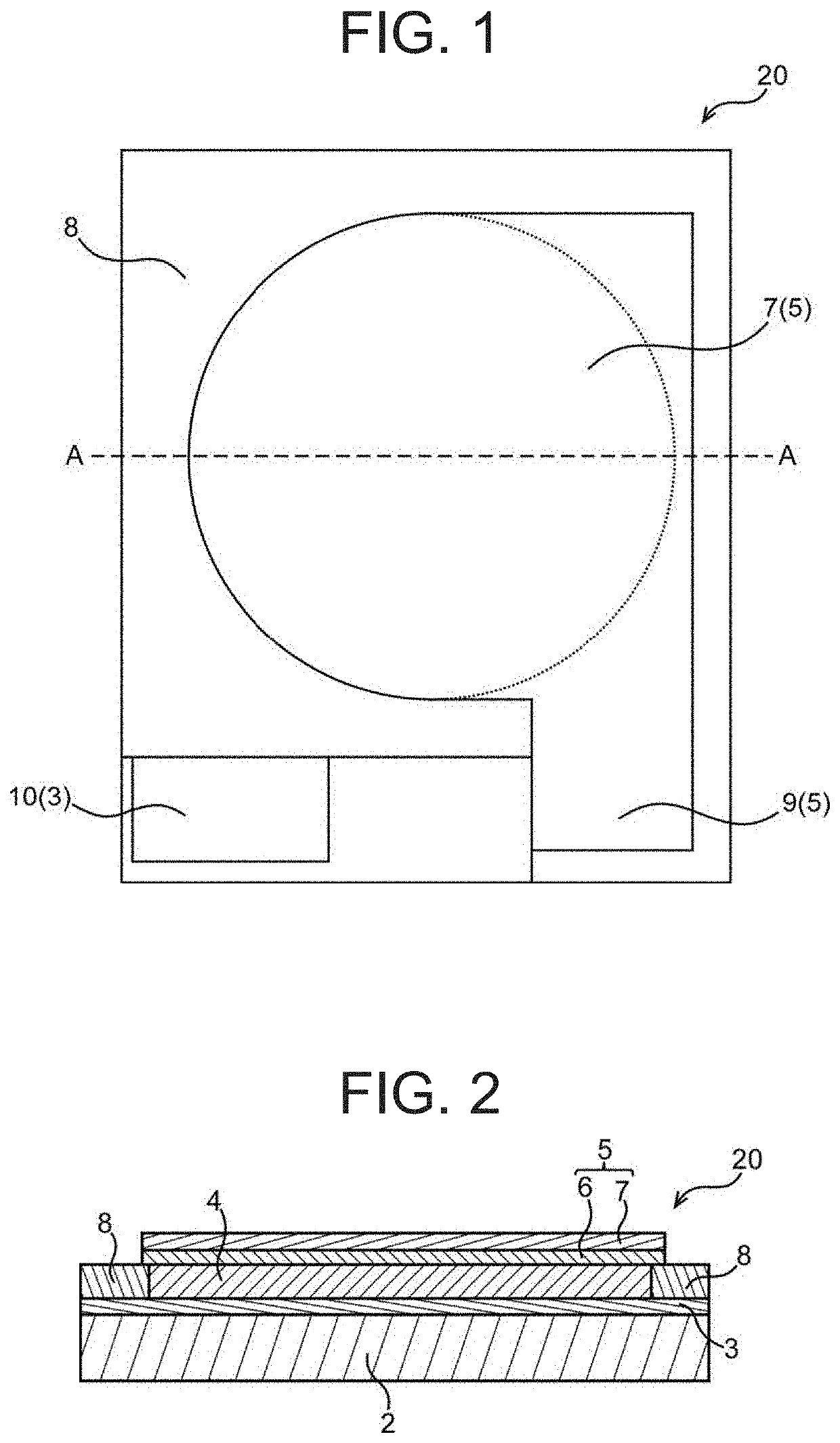
[0031]FIG. 1 is a schematic top view of an electron emission element of this embodiment, and FIG. 2 is a schematic sectional view of the electron emission element taken along a broken line A-A of FIG. 1.
[0032]The electron emission element 20 of this embodiment includes a lower electrode 3, a surface electrode 5, and a silicone resin layer 4 disposed between the lower electrode 3 and the surface electrode 5, the surface electrode 5 includes a silver layer 6, and the silver layer 6 is in contact with the silicone resin layer 4.
[0033]The electron emission element 20 of this embodiment can have an insulating layer 8 having an opening that defines an electron emission region of the electron emission element 20.
[0034]The electron emission element 20 is an element that emits electrons from the electron emission region of the surface electrode 5 into air, gas, a reduced pressure atmosphere, and the like. The electrons emitted from the electron emission region charge gas to generate anions i...
second embodiment
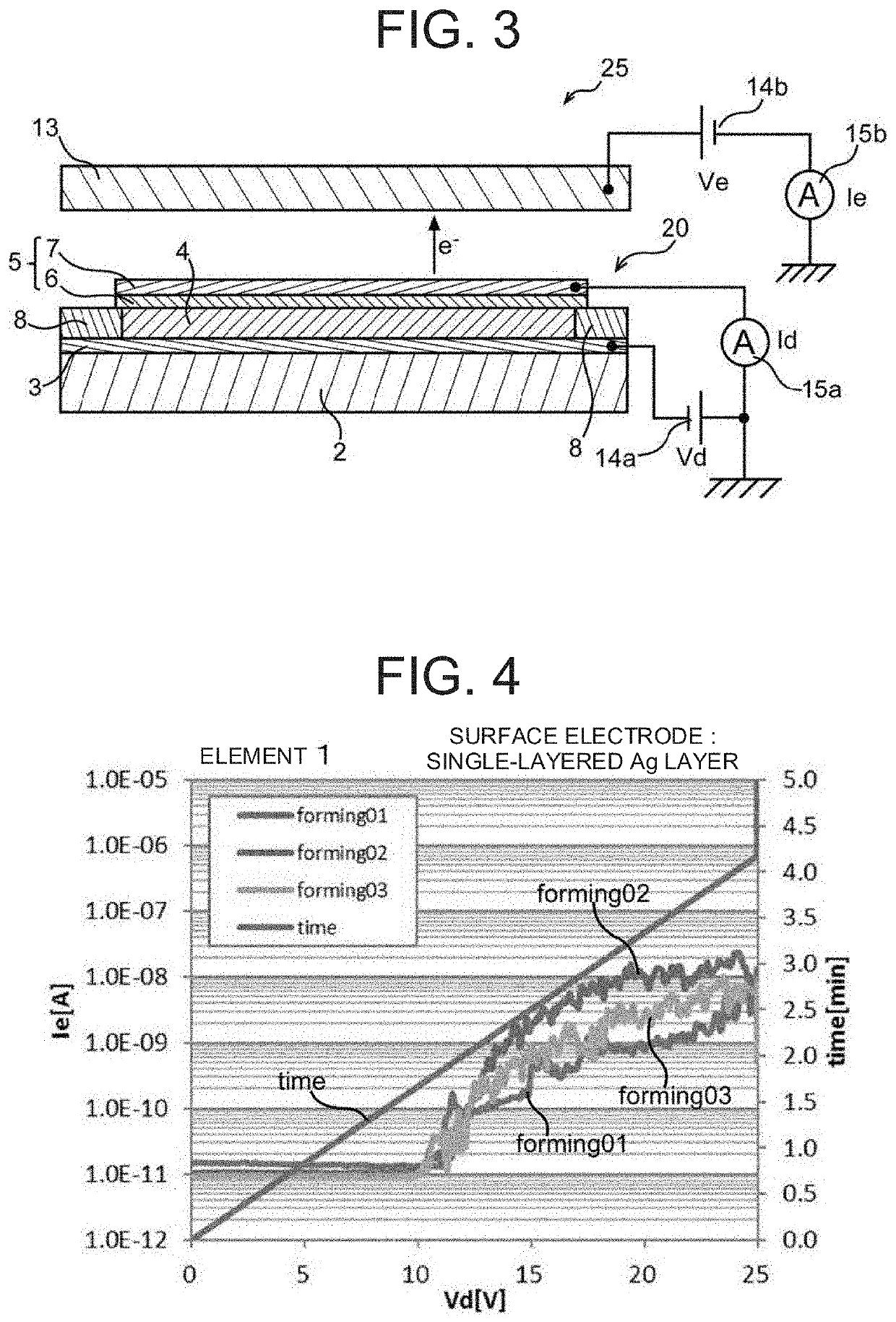
[0055]FIG. 3 is a schematic sectional view of an electron emission device of this embodiment. FIG. 3 also illustrates a circuit diagram illustrating an electrical configuration of the electron emission device.
[0056]The electron emission device 25 of this embodiment includes an electron emission element 20, an electric field generating electrode 13, and power supplies 14a and 14b. The power supply 14a is provided so as to apply a voltage between a lower electrode 3 and a surface electrode 5. The power supply 14b is provided so as to apply a voltage between the electron emission element 20 and the electric field generating electrode 13.
[0057]Further, the electron emission device 25 can include an ammeter 15a provided to so as to measure a current that flows between the lower electrode 3 and the surface electrode 5, or an ammeter 15b provided so as to measure a current caused to flow by electrons that are emitted from the electron emission element 20 and that reach the electric field g...
PUM
 Abstract
Description
Claims
Application Information


