Reflective mask blank, reflective mask, and process for producing reflective mask blank

a technology of reflective masks and mask blanks, applied in the field of reflective mask blanks and reflective masks, can solve the problems of telecentricity errors, the position of the image undesirably shifting in a horizontal direction, and the dioptric system used in conventional exposure techniques cannot be used therewith, so as to reduce the effect of mask 3d effects

Pending Publication Date: 2021-11-11
ASAHI GLASS CO LTD
View PDF0 Cites 0 Cited by
  • Summary
  • Abstract
  • Description
  • Claims
  • Application Information

AI Technical Summary

Benefits of technology

[0060]The reflective mask blank of the present invention and the reflective mask obtained from the reflective mask blank can reduce mask 3D effects.

Problems solved by technology

EUV light is apt to be absorbed by many substances and, hence, the dioptric systems used in conventional exposure techniques cannot be used therewith.
In this case, if the position of the wafer shifts upward or downward from the focal plane, the position of the image undesirably shifts in a horizontal direction.
This is called a telecentricity error.
In this case, thinning the absorbent layer is insufficient in reducing the mask 3D effects.
This method, however, has a dependence on pattern pitch and has not succeeded in reducing the telecentricity error in all patterns differing in pitch.

Method used


Image

  • Reflective mask blank, reflective mask, and process for producing reflective mask blank
  • Reflective mask blank, reflective mask, and process for producing reflective mask blank
  • Reflective mask blank, reflective mask, and process for producing reflective mask blank

Examples


example 1

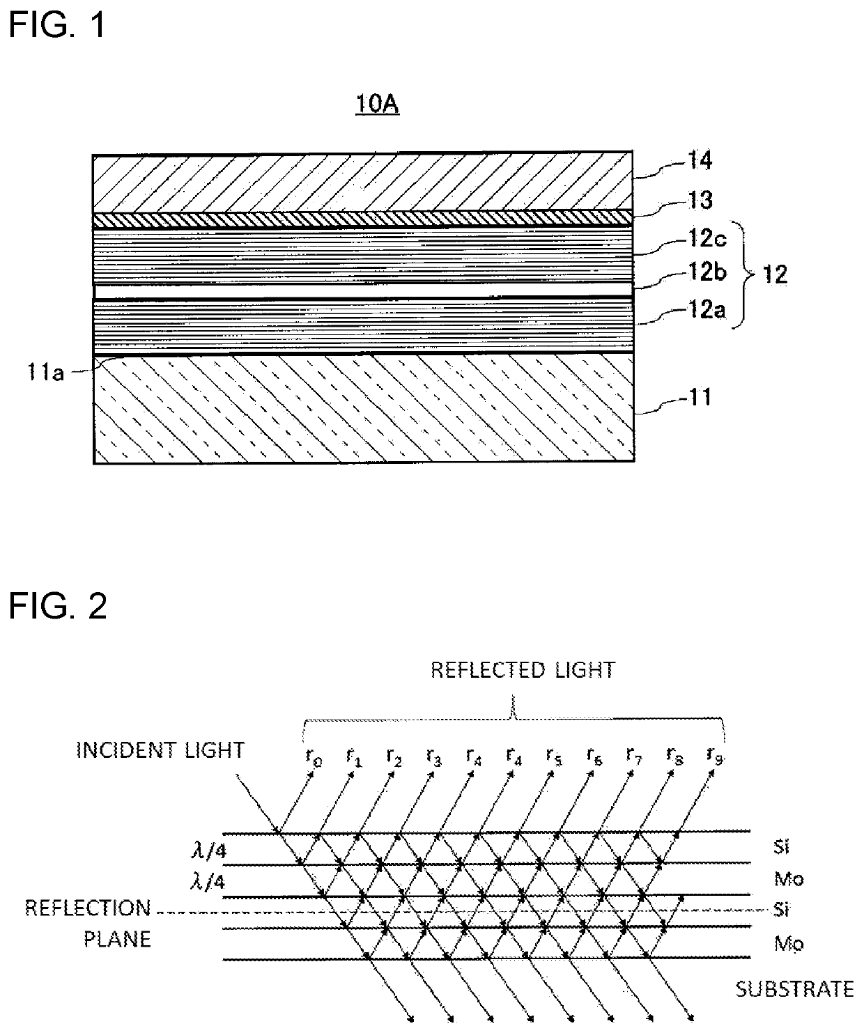
[0136]A reflective mask blank 10D is shown in FIG. 13. The reflective mask blank 10D includes a reflective layer 12 having no phase inversion layer 12b therein.

(Production of Reflective Mask Blank)

[0137]As a substrate 11 for deposition, an SiO2—TiO2 glass substrate (outer shape, about 152-mm square; thickness, about 6.3 mm) was used. This glass substrate had a coefficient of thermal expansion of 0.02×10⁻⁷ / ° C. or less. The glass substrate was polished to make a surface thereof flat and have a surface roughness of 0.15 nm or less in terms of root-mean-square roughness Rq and a flatness of 100 nm or less. A Cr layer having a thickness of about 100 nm was deposited on the back surface of the glass substrate by magnetron sputtering, thereby forming a backside electroconductive layer 16 for electrostatic chucking. The Cr layer had a sheet resistance value of about 100 Ω / □.

[0138]After the deposition of the backside electroconductive layer 16 on the back surface of the substrate 11, an Si ...

example 2

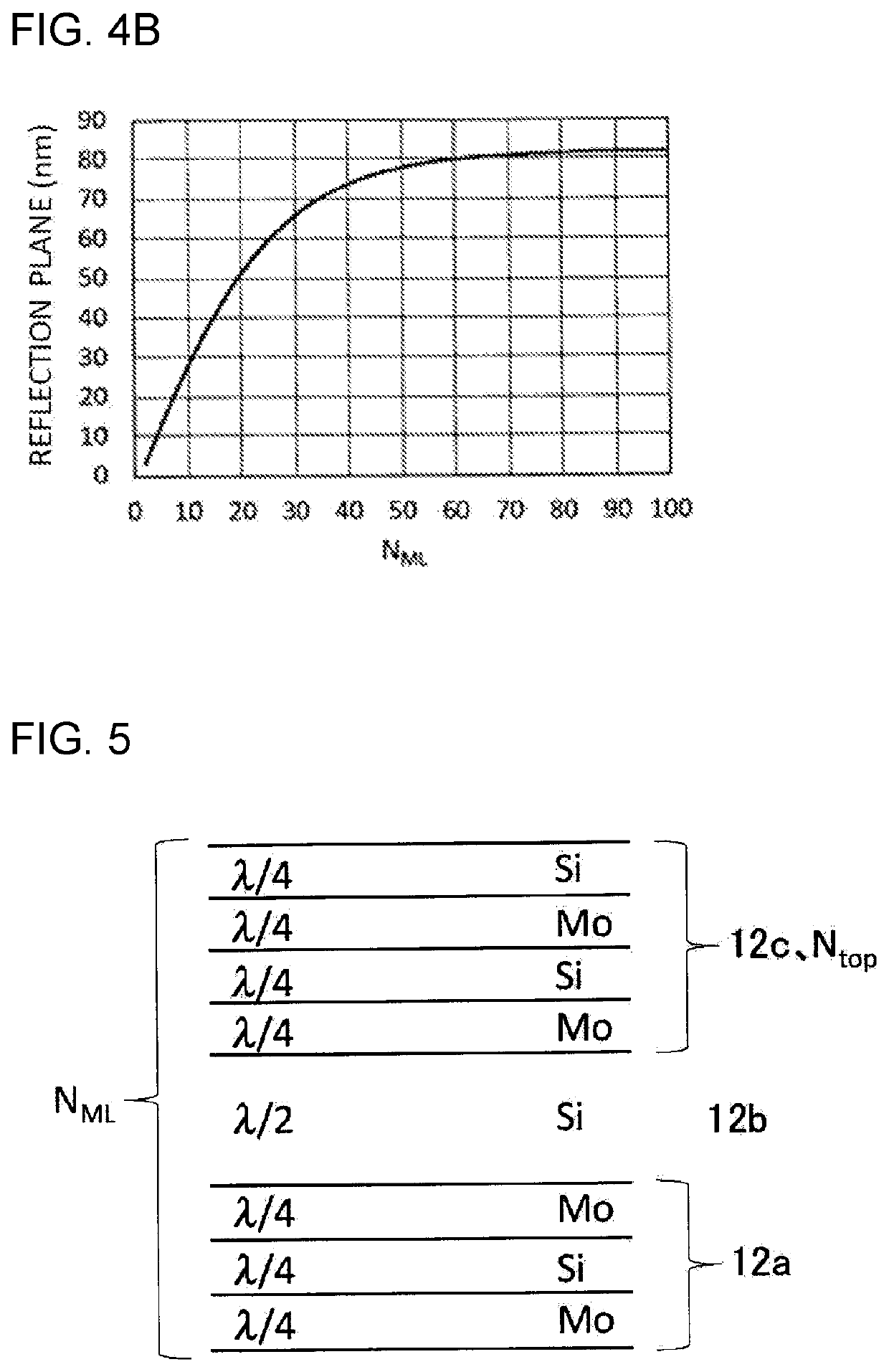
[0145]In this Example, the reflective mask blank 10C shown in FIG. 9 is produced. The reflective mask blank 10C includes a reflective layer 12 having a phase inversion layer 12b therein. The reflective layer 12 is configured by superposing a lower multilayer film 12a, the phase inversion layer 12b, and an upper multilayer film 12c in this order from the substrate 11 side.

(Production of Reflective Mask Blank)

[0146]This Example differs from Example 1 in the method for forming the reflective layer 12. A substrate 11, a backside electroconductive layer 16, a protective layer 13, and an absorbent layer 14 were produced by the same methods as in Example 1.

[0147]After the deposition of the backside electroconductive layer 16 on the back surface of the substrate 11, an Si film and an Mo film were alternately deposited repeatedly over 15 cycles on the front surface of the substrate 11 by ion-beam sputtering. The film thickness of each Si film was about 4.0 nm and the film thickness of each M...

example 3

[0157]In this Example, the reflective mask blank 10C shown in FIG. 9 is produced as in Example 2. This Example differs from Example 2 in the number of layers of the lower multilayer film 12a, the number of layers Ntop of the upper multilayer film 12c, and the total number of layers NML of the reflective film 12.

(Production of Reflective Mask Blank)

[0158]After a backside electroconductive layer 16 had been deposited on the back surface of a substrate 11, an Si film and an Mo film were alternately deposited repeatedly over 30 cycles on the front surface of the substrate 11 by ion-beam sputtering. The film thickness of each Si film was about 4.0 nm and the film thickness of each Mo film was about 3.0 nm. Thus, a lower multilayer film 12a having an overall film thickness of about 210 nm ((4.0 nm of Si film)+(3.0 nm of Mo film)×30) was formed.

[0159]The uppermost surface of the lower multilayer film 12a was an Mo film. An Si film serving as a phase inversion layer 12b was deposited thereo...


PUM

PropertyMeasurementUnit
thicknessaaaaaaaaaa
wavelengthsaaaaaaaaaa
wavelengthaaaaaaaaaa

Abstract

A reflective mask blank includes a substrate and, disposed on or above the substrate in the following order from the substrate side, a reflective layer, a protective layer, and an absorbent layer. The reflective layer is a multilayered reflective film includes a plurality of cycles, each cycle including a high-refractive-index layer and a low-refractive-index layer. The reflective layer includes one phase inversion layer which is either the high-refractive-index layer or the low-refractive-index layer each having a film thickness increased by Δd ([unit: nm]). The increase in film thickness Δd [unit: nm] of the phase inversion layer satisfies a relationship: (¼+m/2)×13.53−1.0≤Δd≤(¼+m/2)×13.53+1.0. The reflective layer and the absorbent layer satisfy a relationship:
Tabs+80 tanh(0.037NML)−1.6 exp(−0.08Ntop)(NML−Ntop)2<140.

Description

CROSS-REFERENCE TO RELATED APPLICATIONS[0001]This is a bypass continuation of International Patent Application No. PCT / JP2020 / 001316, filed on Jan. 16, 2020, which claims priority to Japanese Patent Application No. 2019-007681, filed on Jan. 21, 2019. The contents of these applications are hereby incorporated by reference in their entireties.TECHNICAL FIELD[0002]The present invention relates to a reflective mask blank, a reflective mask, and a process for producing the reflective mask blank.BACKGROUND ART[0003]Nowadays, with the progress of microfabrication of integrated circuits for constituting semiconductor devices, extreme ultraviolet (hereinafter referred to as “EUV”) lithography is being investigated as an exposure method which replaces the conventional exposure technique employing visible light or ultraviolet light (wavelengths, 365-193 nm).[0004]In EUV lithography, EUV light is used as a light source for exposure. The term “EUV light” means light having a wavelength in the s...

Claims


Application Information

Patent Timeline
Patent Type & Authority Applications(United States)
IPC IPC(8): G03F1/24G03F1/52
CPCG03F1/24G03F1/52
Inventor TANABE, HIROYOSHIMIYAGI, TAKAHIRA
Owner ASAHI GLASS CO LTD
Why Eureka
Try Eureka