On-chip antenna and on-chip antenna array

a technology of antenna array and silicon substrate, which is applied in the direction of individual energised antenna array, resonant antenna, array feeding system, etc., can solve the problems of narrow bandwidth and low antenna gain of prior art on-chip antennas, and achieve high permittivity and high contrast of permittivity

Pending Publication Date: 2021-12-02
CITY UNIVERSITY OF HONG KONG
View PDF5 Cites 2 Cited by
  • Summary
  • Abstract
  • Description
  • Claims
  • Application Information

AI Technical Summary

Benefits of technology

[0008]Prior art on-chip antennae suffer from narrow bandwidth and low antenna gain. However, the invention provides a possibility of mitigating these two problems, by the combination of a dipole mode and a dielectric resonator mode. Such an on-chip antenna provides a possibility of overall system size and cost reduction and, it provides a possibility of eliminating matching network and parasitic due to wire bonding when compared to off-chip antennae.
[0012]Preferably the dipole antenna comprises at least one comb shaped dipole element, the comb shaped dipole element comprising a base and a plurality of substantially parallel fingers extending from the base. Advantageously, use of a comb-shaped dipole element provides a possibility of reducing the cross polarization level.

Problems solved by technology

Prior art on-chip antennae suffer from narrow bandwidth and low antenna gain.

Method used


Image

  • On-chip antenna and on-chip antenna array
  • On-chip antenna and on-chip antenna array
  • On-chip antenna and on-chip antenna array

Examples


Embodiment Construction

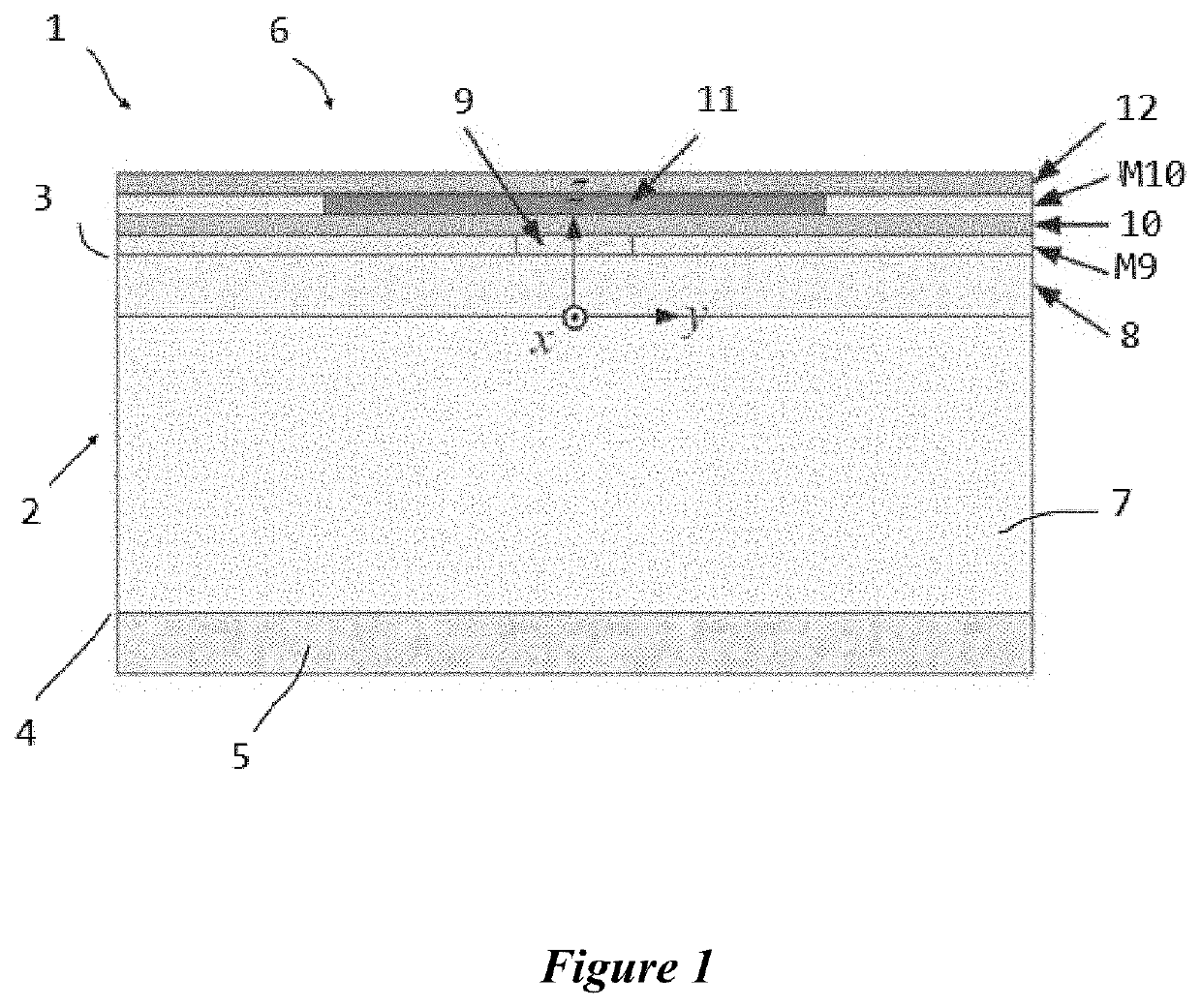
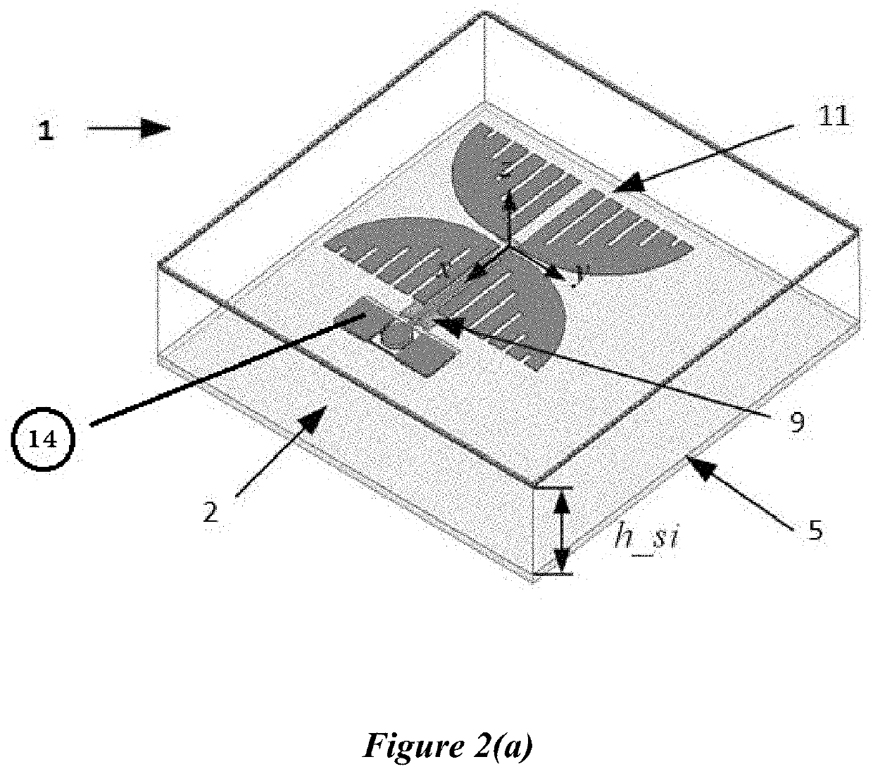
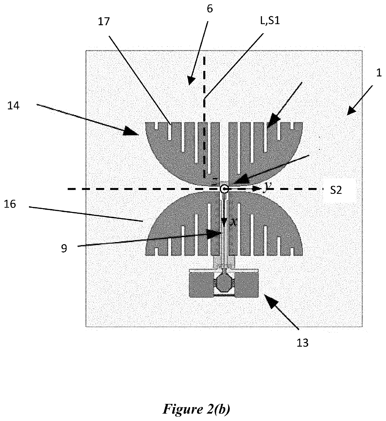
[0040]Shown in FIG. 1 is a first embodiment of an on-chip antenna 1 according to the invention in vertical cross section. The on-chip antenna 1 is a linearly polarised antenna 1 comprising a substrate 2 which in turn comprises first and second faces 3,4. Arranged on the second face 4 is a metal layer 5. Arranged on the first face 3 is a dipole antenna structure 6. The substrate 2 comprises a silicon layer 7 and a silicon dioxide layer 8 with the dipole antenna structure 6 arranged on the silicon dioxide layer 8 and the metal layer 5 arranged on the silicon layer 7.

[0041]The dipole antenna structure 6 comprises a feed structure 9, in this case a coplanar waveguide line 9, formed in a metal layer M9 on the silicon dioxide layer 8. Arranged on layer M9 is passivation layer 10. The dipole antenna structure 6 further comprises a dipole antenna 11 formed in a further metal layer M10 arranged on the passivation layer 10. Arranged on metal layer M10 is a further passivation layer 12. The di...


PUM


Abstract

An on-chip antenna comprising an electrically insulating substrate having first and second faces; a metal layer arranged on the second face; and, a dipole antenna structure arranged on the first face, the dipole antenna structure comprising a dipole antenna and a feed structure connected to the dipole antenna; the on-chip antenna being configured such that when the feed structure is fed with an electrical signal it operates simultaneously in (i) at least one dielectric resonator mode to function as a dielectric resonance antenna, and (ii) at least one dipole mode to function as a cavity backed dipole antenna.

Description

BACKGROUND OF THE INVENTION[0001]The present invention relates to an on-chip antenna. More particularly, but not exclusively, the present invention relates to an on-chip antenna comprising a substrate having first and second faces, a metal layer on the second face and a dipole antenna structure on the first face, wherein the on-chip antenna is configured to operate simultaneously in at least one dielectric resonator mode and at least one dipole mode to function as a cavity backed dipole antenna.[0002]The present invention also relates to an on-chip antenna array. More particularly, but not exclusively the present invention relates to an on-chip antenna array comprising: a plurality of on-chip antennae arranged on a common base layer in an n*m array, each substrate being separated from an adjacent substrate by a separator that has a dielectric permittivity lower than that of the substrates.[0003]The present invention also relates to an integrated circuit comprising: at least one of a...

Claims


Application Information

Patent Timeline
Patent Type & Authority Applications(United States)
IPC IPC(8): H01Q21/00H01Q9/28H01Q9/04H01Q1/22H01Q21/06
CPCH01Q21/0025H01Q9/285H01Q21/062H01Q1/2283H01Q9/0485H01Q9/0457H01Q5/15H01Q1/523
Inventor CHAN, CHI HOUKONG, SHANG CHENGSHUM, KAM MAN
Owner CITY UNIVERSITY OF HONG KONG
Why Eureka
Try Eureka