Quantum device
- Summary
- Abstract
- Description
- Claims
- Application Information
AI Technical Summary
Benefits of technology
Problems solved by technology
Method used
Image

Examples
first example embodiment
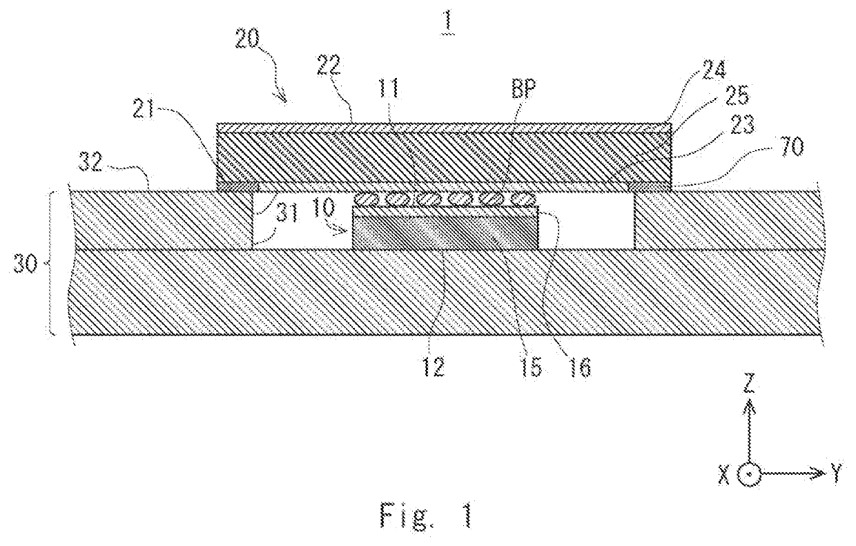
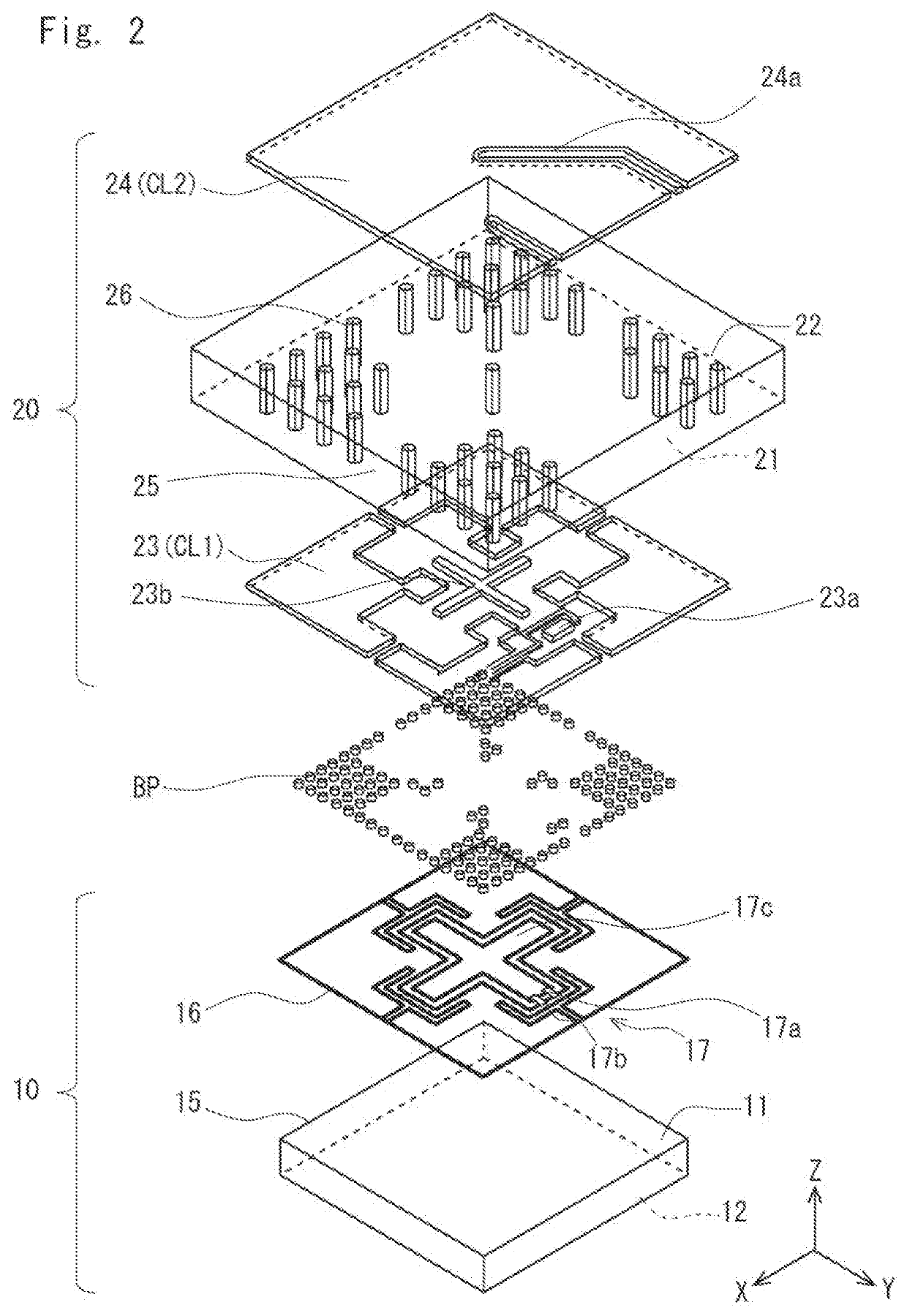
[0033]A quantum device according to a first example embodiment will be described. FIG. 1 is a cross-sectional view showing an example of a quantum device according to the first example embodiment. FIG. 2 is an exploded perspective view showing an example of a quantum chip and an interposer in the quantum device according to the first example embodiment. As shown in FIGS. 1 and 2, the quantum device 1 includes a quantum chip 10 and an interposer 20.
[0034]The quantum chip 10 includes a chip substrate 15 and a wiring layer 16. The chip substrate 15 contains, for example, silicon (Si). Note that the chip substrate 15 is not limited to those containing silicon and may include those containing other electronic materials such as sapphire or a compound semiconductor material (Groups IV, III-V, and II-VI) as long as the quantum chip 10 can form a quantum bit. Further, the material is preferably a single-crystalline material, but it may be a polycrystalline material or an amorphous material.
[...
first modified example
[0074]Next, a first modified example of the first example embodiment will be described. This modified example includes a bonding layer or a junction layer between the quantum chip 10 and the sample stage 30. FIG. 10 is a cross-sectional view showing an example of a bonding layer or a junction layer according to a first modified example of the first example embodiment. As shown in FIG. 10, in a quantum device la according to the first modified example, at least a part of the second surface 12 of the quantum chip 10 may be bonded or joined to the inner surface of the recessed part 31 of the sample stage 30. For example, the second surface 12 may be bonded to a predetermined surface 32 of the sample stage 30, such as the upper surface thereof, by a bonding layer BL made of varnish, grease, or the like. Further, the second surface 12 may be joined by the sample stage 30 by using a junction layer ML, which is, for example, a metal layer, formed between the chip substrate 15 and the sampl...
second modified example
[0077]Next, a second modified example of the first example embodiment will be described. In this modified example, there is a space between the quantum chip 10 and the sample stage 30. FIG. 11 is a cross-sectional view showing an example of a space between the quantum chip 10 and the sample stage 30 according to the second modified example of the first example embodiment. As shown in FIG. 11, in a quantum device 1b according to the second modified example, the quantum chip 10 does not have to be in contact with the sample stage 30. That is, the second surface 12 of the quantum chip 10 may be disposed in such a manner that a space is formed between the second surface 12 and the inner surface of the recessed part 31 of the sample stage 30. By the above-described configuration, it is possible to reduce the stress and the strain caused by the difference between the thermal contraction of the quantum chip 10 caused by the change of the temperature to an extremely low temperature and that...
PUM
 Abstract
Description
Claims
Application Information
 - R&D Engineer
- R&D Manager
- IP Professional
- Industry Leading Data Capabilities
- Powerful AI technology
- Patent DNA Extraction
Browse by: Latest US Patents, China's latest patents, Technical Efficacy Thesaurus, Application Domain, Technology Topic.
© 2024 PatSnap. All rights reserved.Legal|Privacy policy|Modern Slavery Act Transparency Statement|Sitemap