Power device with high-voltage radio-frequency lateral diffusion structure and production method of power device

A power device and diffusion structure technology, which is applied in semiconductor/solid-state device manufacturing, electric solid-state devices, semiconductor devices, etc., can solve the problems of gate oxide layer quality degradation, high resistivity of tungsten silicon, poor reliability, etc., to avoid source and the effect of drain shorting

Active Publication Date: 2012-05-09
ADVANCED SEMICON MFG CO LTD
View PDF3 Cites 13 Cited by
  • Summary
  • Abstract
  • Description
  • Claims
  • Application Information

AI Technical Summary

Problems solved by technology

[0003] The resistance of polycrystalline gate is a very important parameter of high-frequency LDNMOS. The traditional polycrystalline silicide is tungsten silicide (WSix). The process is simple, but the resistivity of tungsten silicon is relatively large (greater than 6ohm / sqr), and the high-stress chemical vapor phase Fluorine, a by-product of deposition (CVD), may diffuse into the gate oxide, degrading the quality of the gate oxide and risking poor reliability

Method used


Image

  • Power device with high-voltage radio-frequency lateral diffusion structure and production method of power device
  • Power device with high-voltage radio-frequency lateral diffusion structure and production method of power device
  • Power device with high-voltage radio-frequency lateral diffusion structure and production method of power device

Examples


Embodiment Construction

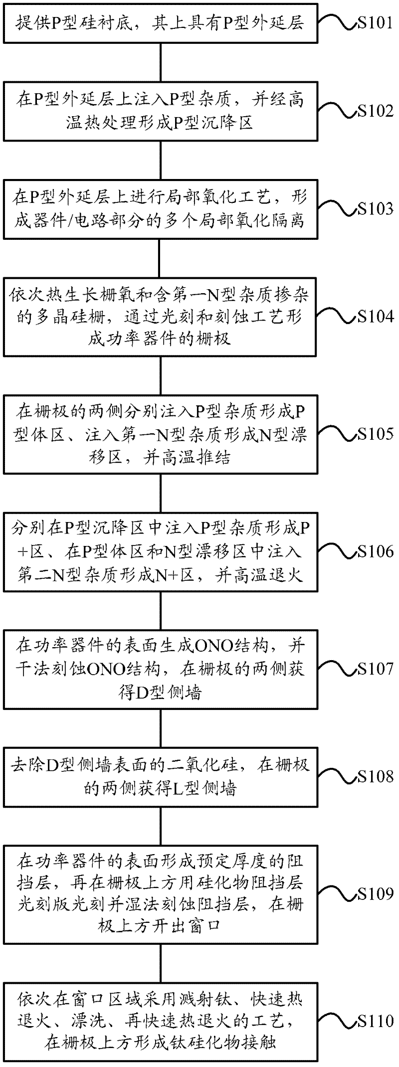
[0057] The present invention will be further described below in conjunction with specific embodiment and accompanying drawing, set forth more details in the following description so as to fully understand the present invention, but the present invention can be implemented in many other modes different from this description obviously, Those skilled in the art can make similar promotions and deductions based on actual application situations without violating the connotation of the present invention, so the content of this specific embodiment should not limit the protection scope of the present invention.

[0058] figure 1 It is a flowchart of a method for manufacturing a power device with a high-voltage radio frequency lateral diffusion structure according to an embodiment of the present invention. like figure 1 As shown, the manufacturing method may include:

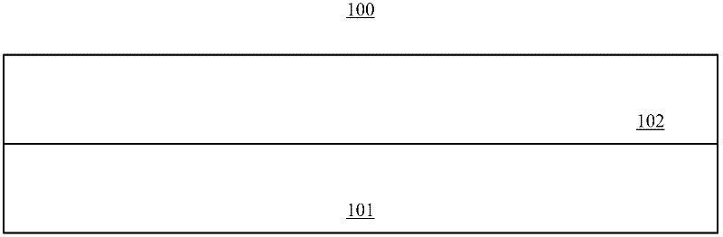
[0059] Executing step S101, providing a P-type silicon substrate on which a P-type epitaxial layer is formed;
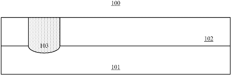
[0060]...


PUM


Abstract

The invention provides a power device with a high-voltage radio-frequency lateral diffusion structure and a production method of the power device. The production method comprises the steps of providing a P-type substrate, on which a P-type epitaxial layer is arranged; forming a P-type depressed region and a plurality of local oxide isolations on the epitaxial layer; thermally growing gate oxide and phosphor-doped polycrystalline silicon gate to form a grid; respectively filling boron on the two sides of the grid to form a P-type body region, filling phosphor to form an N-type drift region, push-connecting the P-type body region with the N-type drift region at high temperature; respectively filling boron in the P-type depressed region to form a P+ region, filling arsenic in the P-type body region and the N-type drift region to form an N+ region and annealing at high temperature; generating an oxide-nitride-oxide (ONO) structure on the surface of a device, etching through a dry process and obtaining D-shaped side walls on the two sides of the grid; removing silicon dioxide on the surfaces of the side walls and obtaining L-shaped side walls; forming a barrier layer on the surface of the device and opening a window above the grid; and forming titanium silicide contact above the grid. The power device with the high-voltage radio-frequency lateral diffusion structure and the production method of the power device have the advantages that the risks that the source is short-circuited with the drain can be effectively avoided, the grid silicide with very low resistivity can be obtained and the demands of high-frequency lateral diffusion metal-oxide-semiconductor field-effect transistors (LDMOS) can be met.

Description

technical field [0001] The invention relates to the technical field of semiconductor device manufacturing, in particular, the invention relates to a power device with a high-voltage radio frequency lateral diffusion structure and a manufacturing method thereof. Background technique [0002] Power devices with high-frequency lateral diffusion structure (Lateral Diffusion MOSFET, LDMOS for short) (frequency range 2.11GHz ~ 2.17GHz, breakdown voltage ≥ 70V, output power 30W) are widely used in 3G communication radio frequency base stations, radar, digital TV, etc. . High-performance high-frequency LDNMOS not only requires high voltage resistance and high drive current, but also has higher requirements for frequency, so the research on its related technology is a hot research field in recent years. [0003] The resistance of polycrystalline gate is a very important parameter of high-frequency LDNMOS. The traditional polycrystalline silicide is tungsten silicide (WSix). The proc...

Claims


Application Information

Patent Timeline
Patent Type & Authority Applications(China)
IPC IPC(8): H01L21/28H01L21/48H01L21/336H01L29/423H01L23/488H01L29/78
CPCH01L2924/0002H01L2924/00
Inventor 青云刘建华
Owner ADVANCED SEMICON MFG CO LTD
Why Eureka
Try Eureka