Light-emitting display unit and display apparatus

a display unit and light-emitting technology, applied in the direction of identification means, semiconductor/solid-state device details, instruments, etc., can solve the problems of high manufacturing cost of organic light-emitting diodes (oled) display panels, difficult to meet the needs of large-area transfer, and low yield of micro light-emitting devices. , to achieve the effect of simplifying circuit layers, improving the yield of transfer (transferring and positioning) of micro light-emitting devices, and light-

Active Publication Date: 2022-02-24
PLAYNITRIDE DISPLAY CO LTD
View PDF1 Cites 0 Cited by
  • Summary
  • Abstract
  • Description
  • Claims
  • Application Information

AI Technical Summary

Benefits of technology

[0026]Based on the above description, in the light-emitting display unit of an embodiment of the invention, the conductive patterns of the first metal layer are electrically connected to the pad patterns of the third metal layer through the transfer patterns of the second metal layer, respectively. Based on the fact that the distribution density of the second metal layer is greater than the distribution density of the first metal layer and the distribution density of the third metal layer, and the distribution density of the first metal layer is greater than the distribution density of the third metal layer, a surface flatness of the light-emitting unit configured with the conductive patterns may be effectively increased, and a transposition (transferring and positioning) yield of the micro light-emitting devices is therefore improved. A plurality of the light-emitting display units are adapted to be electrically connected to the printed circuit board through the respective pad patterns to form a display apparatus. The pre-made light-emitting display units may s

Problems solved by technology

In recent years, under the situation that manufacturing cost of organic light-emitting diode (OLED) display panel is too high and a service life thereof cannot compete with current mainstream displays, micro LED displays have gradually attracted investment attentions of major technology manufacturers.
Therefore, it is hard to meet the needs of large

Method used


Image

  • Light-emitting display unit and display apparatus
  • Light-emitting display unit and display apparatus
  • Light-emitting display unit and display apparatus

Examples


Embodiment Construction

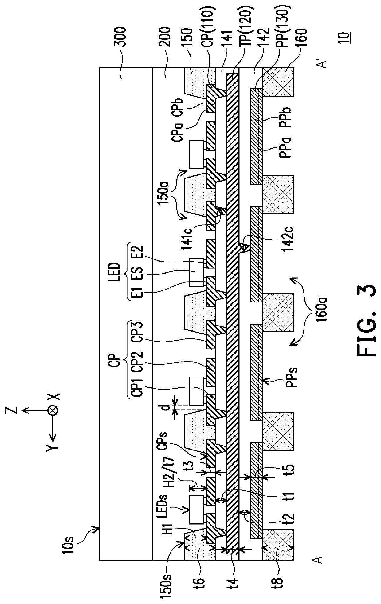
[0037]In the drawings, thicknesses of layers, films, panels, regions, etc., are exaggerated for clarity's sake. It should be noted that when an element such as a layer, a film, a region, or a substrate is referred to as being “on” or “connected” to another element, the element may be directly on or connected to the other element, or an intermediate element may exist. In contrast, when an element is referred to as being “directly on” or “directly connected to” another element, no intermediate element exists. As used herein, “connection” may refer to physical and / or electrical connection. Furthermore, “electrical connection” means that there may be other components between two components.

[0038]Reference will now be made in detail to the present preferred embodiments of the invention, examples of which are illustrated in the accompanying drawings. Wherever possible, the same reference numbers are used in the drawings and the description to refer to the same or like parts.
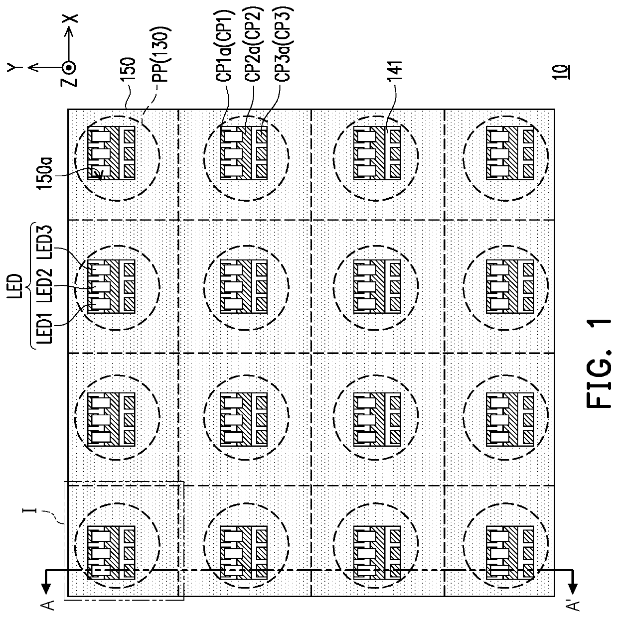
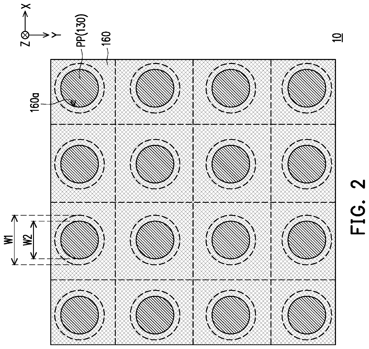
[0039]FIG. 1 i...


PUM


Abstract

A light-emitting display unit including first to third metal layers, first to second insulation layers and micro light-emitting devices is provided. The first metal layer has conductive patterns. The second metal layer has transfer patterns. The third metal layer has pad patterns. The second metal layer is located between the first metal layer and the third metal layer. A distribution density of the first metal layer is less than that of the second metal layer, and greater than that of the third metal layer. The first insulation layer is disposed between the first metal layer and the second metal layer. The second insulation layer is disposed between the second metal layer and the third metal layer. The micro light-emitting devices are disposed on one side of the first metal layer away from the second metal layer, and electrically bonded to the conductive patterns. A display apparatus adopting the light-emitting display unit is also provided.

Description

CROSS-REFERENCE TO RELATED APPLICATION[0001]This application claims the priority benefits of U.S. provisional application Ser. No. 63 / 069,693, filed on Aug. 24, 2020, and Taiwan application serial no. 109146585, filed on Dec. 29, 2020. The entirety of each of the above-mentioned patent applications is hereby incorporated by reference herein and made a part of this specification.BACKGROUNDTechnical Field[0002]The invention relates to a self-luminous display technology, and particularly relates to a light-emitting display unit and a display apparatus.Description of Related Art[0003]In recent years, under the situation that manufacturing cost of organic light-emitting diode (OLED) display panel is too high and a service life thereof cannot compete with current mainstream displays, micro LED displays have gradually attracted investment attentions of major technology manufacturers. The micro LED display has optical performance equivalent to an OLED display technology, such as high color ...

Claims


Application Information

Patent Timeline
IPC IPC(8): H01L25/075H01L33/62
CPCH01L25/0753H01L24/16H01L33/62G09F9/33G09G3/32H01L2224/16225H01L2224/13101H01L2224/81801H01L24/97H01L24/81H01L24/13H01L2924/181H01L2924/12041H01L25/167H01L2924/014H01L2924/00014H01L2924/00012H01L23/49816H01L27/156H01L33/486H01L33/60H01L2224/16227H01L24/18H01L24/26
Inventor SU, PO-JENLIN, WEI-PING
Owner PLAYNITRIDE DISPLAY CO LTD
Why Eureka
Try Eureka