Micro semiconductor structure and manufacturing method thereof
- Summary
- Abstract
- Description
- Claims
- Application Information
AI Technical Summary
Benefits of technology
Problems solved by technology
Method used
Image

Examples
Embodiment Construction
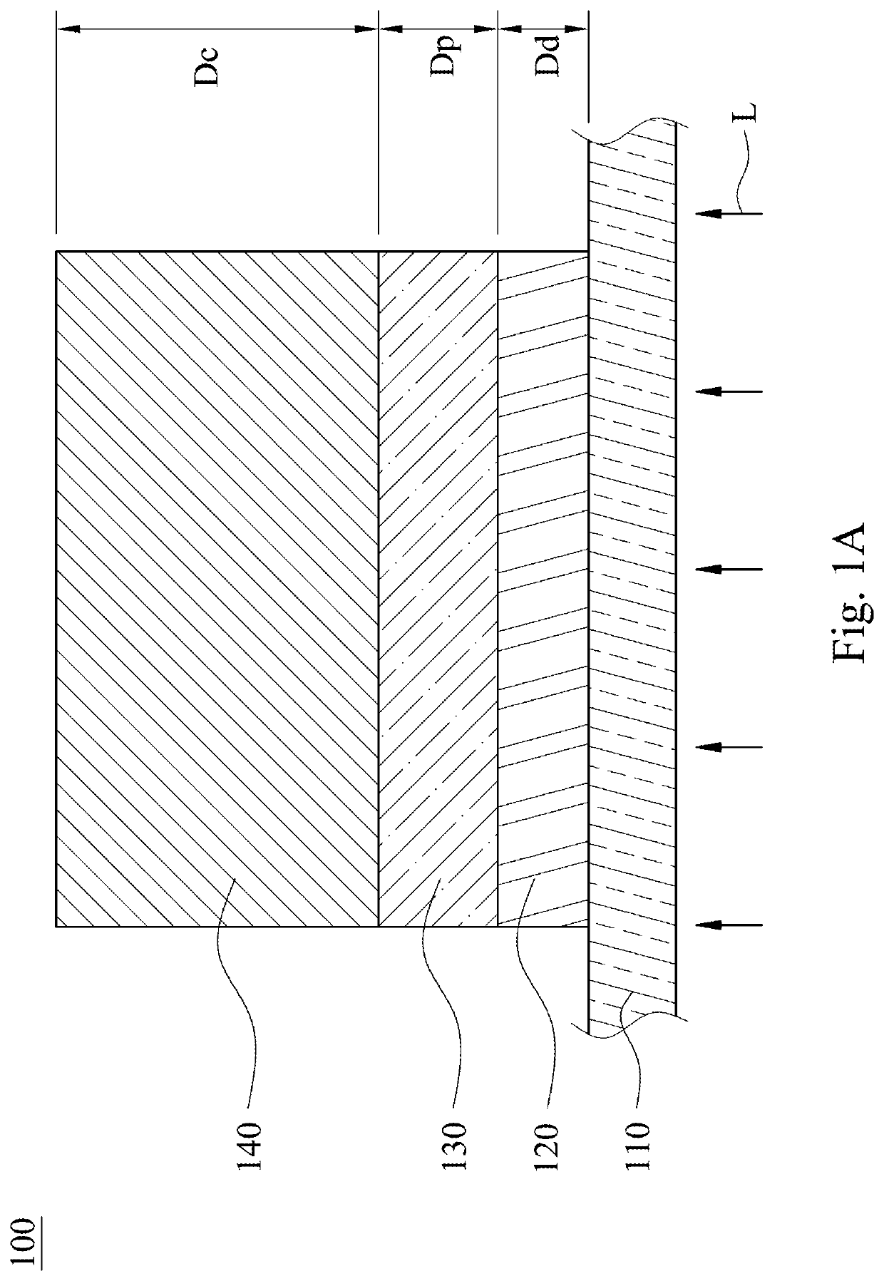
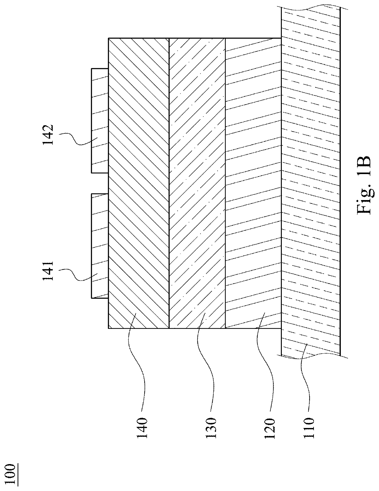
[0021]FIG. 1A is a schematic view of a micro semiconductor structure 100 according to one example of the 1st embodiment of the present disclosure. As shown in FIG. 1A, the micro semiconductor structure 100 includes a substrate 110, a dissociative layer 120, a protective layer 130, and a micro semiconductor 140, wherein the dissociative layer 120, the protective layer 130, and the micro semiconductor 140 are disposed on the substrate 110 in order.
[0022]In detail, according to the 1st embodiment, the dissociative layer 120 is located on one side of the substrate 110 and is disposed on the substrate 110. The dissociative layer 120 is made of a photo-dissociative material, which can be dissociated by the irradiation of a light source L (which wavelength is between 240 nm to 360 nm) during the manufacturing of the micro semiconductor structure 100, so that the structures thereon, such as the protective layer 130 and the micro semiconductor 140 can be detached from the substrate 110 and t...
PUM
 Abstract
Description
Claims
Application Information
 - R&D Engineer
- R&D Manager
- IP Professional
- Industry Leading Data Capabilities
- Powerful AI technology
- Patent DNA Extraction
Browse by: Latest US Patents, China's latest patents, Technical Efficacy Thesaurus, Application Domain, Technology Topic.
© 2024 PatSnap. All rights reserved.Legal|Privacy policy|Modern Slavery Act Transparency Statement|Sitemap