Transistor structure with metal interconnection directly connecting gate and drain/source regions

a technology of transistors and metal interconnections, applied in the direction of semiconductor devices, semiconductor/solid-state device details, electrical apparatus, etc., can solve the problems of not being able to shrink proportionally, the area size of those transistors is dramatically increased, etc., to reduce the misalignment issue, reduce the light diffraction effect and reduce the effect of photons

Pending Publication Date: 2022-03-10
ETRON TECH INC +1
View PDF1 Cites 6 Cited by
  • Summary
  • Abstract
  • Description
  • Claims
  • Application Information

AI Technical Summary

Benefits of technology

[0008]The present invention can reduce the photolithography process sensitivity and the misalignment issue between the contact hole and the gate / source / drain regions. Furthermore, the present invention provides one dimensional mask pattern (such as, stripe shape) to reduce the misalignment issue derived from two dimensional mask patterns for small contact hole openings, and also reduce both the light diffraction effect and less photons into small contact-hole problem of the traditional process flow. The transistor structure includes a semiconductor substrate, agate structure, a channel region, and a first conductive region. The semiconductor substrate has a semiconductor surface. The gate structure is above the semiconductor surface, and a first concave is formed to reveal the gate structure. The channel region is under the semiconductor surface. The first conductive region is electrically coupled to the channel region, and a second concave is formed to reveal the first conductive region. Moreover, a mask pattern in a photolithography process is used to define the first concave, and the mask pattern only defines one dimension length of the first concave.

Problems solved by technology

As the shrink of the minimum feature size or technology process node to some nanometer scale, those expensive EUV equipment, complicated etching technologies, exhausted contact-hole openings of the contact mask and extreme tight design rules are required to avoid or to accommodate the misalignments between those contact holes and the gate / drain / source of the transistor.
Therefore, the manufacture cost of those transistors are dramatically increased and the area size of those transistors could not be shrunk proportionally when the minimum feature size or the technology process node is shrunk.
Therefore, how to effectively scale down a size of the MOSFET to integrate more MOSFETs within a planar area of the silicon wafer has become an important issue for a designer of the MOSFET.

Method used


Image

  • Transistor structure with metal interconnection directly connecting gate and drain/source regions
  • Transistor structure with metal interconnection directly connecting gate and drain/source regions
  • Transistor structure with metal interconnection directly connecting gate and drain/source regions

Examples


Embodiment Construction

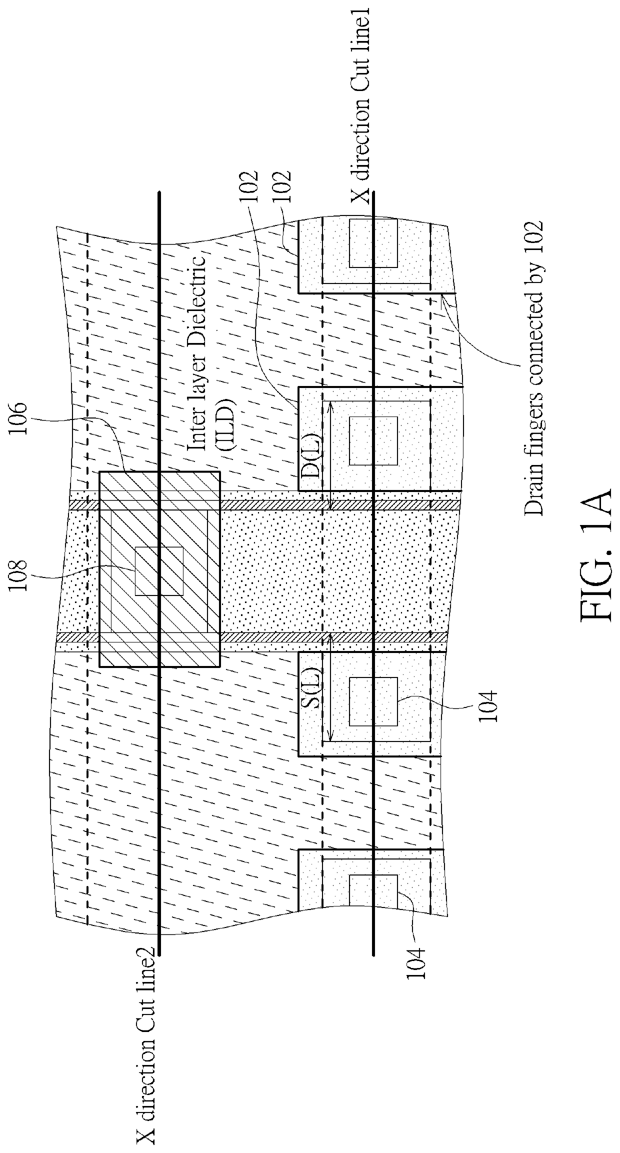
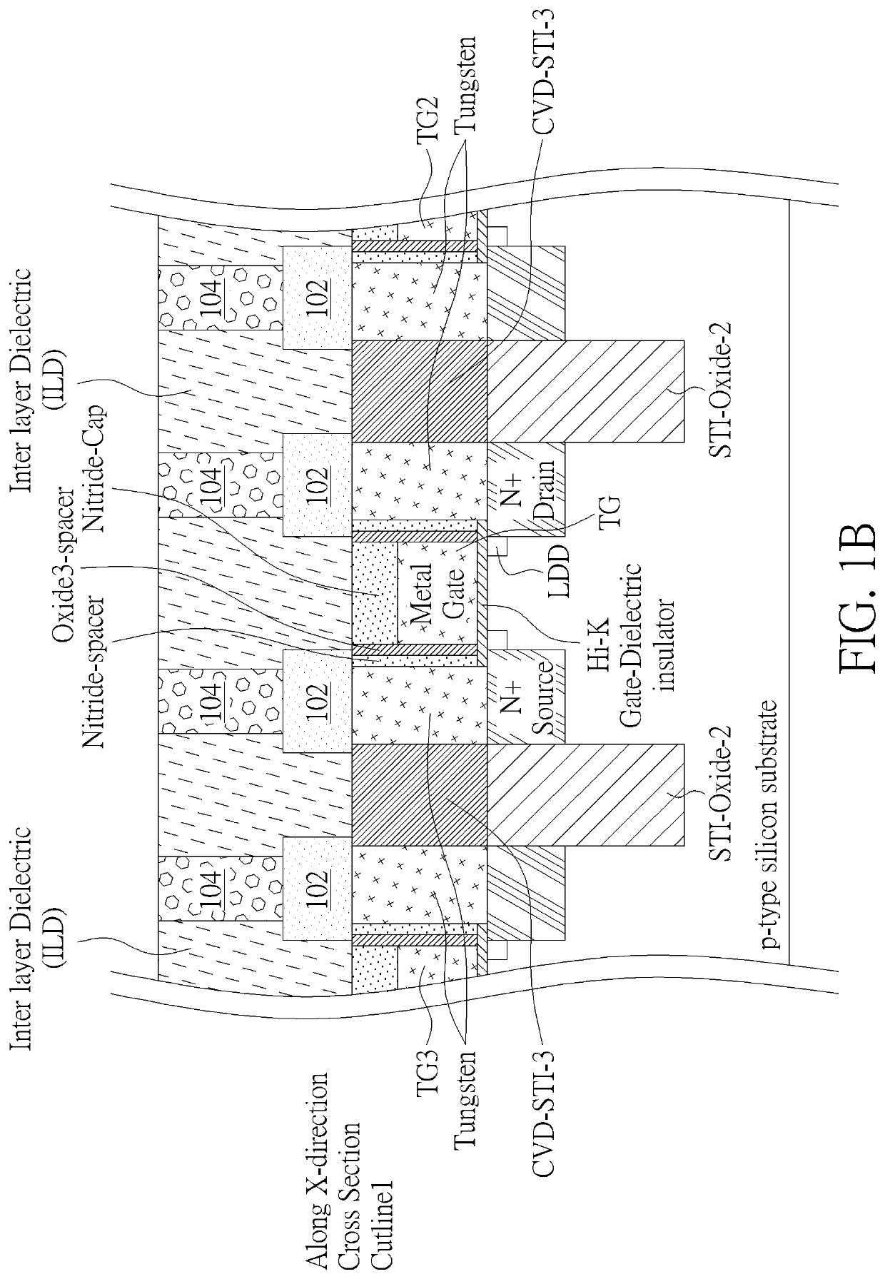
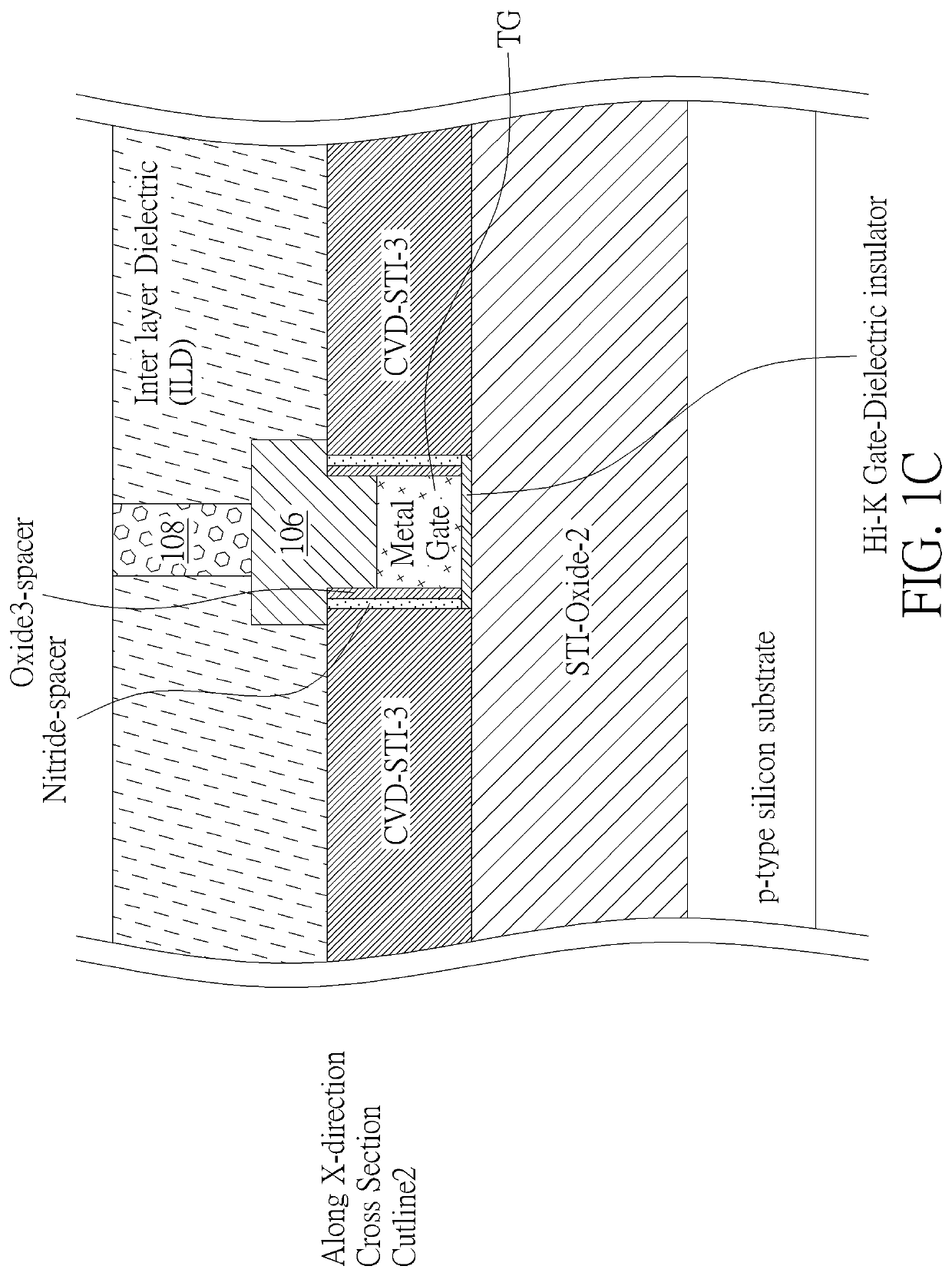
[0086]FIG. 1D is a diagram illustrating a top view of a new MOSFET which is given a name as mMOSFET (miniaturized metal oxide semiconductor field effect transistor) 100 according to an embodiment of the present invention. The mMOSFET 100 especially focuses on a new design to make contact-hole openings on an extension area of a gate structure 101 and on both source region 103 and drain region 107. The gate structure 101 and channel region of the mMOSFET 100 can use either a tri-gate or fin field effect transistor (FinFET) structure or a planar structure, and the source region 103 / the drain region 107 of the mMOSFET 100 can use either n-type dopants for an NMOS transistor or p-type dopants for a PMOS transistor, respectively. In the following description, the present invention utilizes an NMOS transistor as an example with a tri-gate design, and the final gate formation can use either the gate-first or the gate-last approach by the prior art design and process without needs to further...


PUM

PropertyMeasurementUnit
lengthaaaaaaaaaa
lengthaaaaaaaaaa
dimension lengthaaaaaaaaaa

Abstract

A transistor structure includes a semiconductor substrate, a gate structure, a channel region, and a first conductive region. The semiconductor substrate has a semiconductor surface. The gate structure is above the semiconductor surface, and a first concave is formed to reveal the gate structure. The channel region is under the semiconductor surface. The first conductive region is electrically coupled to the channel region, and a second concave is formed to reveal the first conductive region. A mask pattern in a photolithography process is used to define the first concave, and the mask pattern only defines one dimension length of the first concave.

Description

Cross Reference To Related Applications[0001]This application claims the benefit of U.S. Provisional Application No. 63 / 075,841, filed on Sep. 9, 2020 and entitled “MOSFET Structure with First Metal Interconnections Directly Connecting Gate and Drain / Source Regions through Self-Aligned Miniaturized Contacts without Using A Conventional Contact-Hole Mask”, the contents of which are incorporated herein by reference.BACKGROUND OF THE INVENTION1. Field of the Invention[0002]The present invention relates to a transistor structure, and particularly to a transistor structure which can have precisely controlled lengths of source / drain regions and contact-opening to effectively shrink a size of the transistor structure.2. Description of the Prior Art[0003]Since design guidelines of scaling down all dimensions of a metal-oxide-semiconductor field-effect transistor (MOSFET) have been disclosed in the paper published by R. Dennard, et al. in 1974, how to shrink a size of a transistor is a major...

Claims


Application Information

Patent Timeline
Patent Type & Authority Applications(United States)
IPC IPC(8): H01L29/78H01L27/088H01L29/10H01L29/06
CPCH01L29/7851H01L29/0649H01L29/1033H01L27/0886H01L23/481H01L29/785H01L29/66795H01L29/41791H01L21/823431H01L21/823475H01L21/823481H01L27/0207H10B10/12H01L21/76802H01L21/76877H01L21/31144H01L21/823437
Inventor LU, CHAO-CHUN
Owner ETRON TECH INC
Why Eureka
Try Eureka