Method of cleaning wafer and wafer with reduced impurities

Pending Publication Date: 2022-03-24
SENIC INC
View PDF4 Cites 0 Cited by
  • Summary
  • Abstract
  • Description
  • Claims
  • Application Information

AI Technical Summary

Benefits of technology

[0008]This Summary is provided to introduce a selection of concepts in a simplified form that are further described below in the Detailed Description. This Summary is not inten

Problems solved by technology

Also, a CMP process is not enough to remove metal impurities that may flow in during a wafer processing operation.
When a subsequent process proceeds,

Method used


Image

  • Method of cleaning wafer and wafer with reduced impurities
  • Method of cleaning wafer and wafer with reduced impurities
  • Method of cleaning wafer and wafer with reduced impurities

Examples


Example

Example 1

Wafer Cleaning

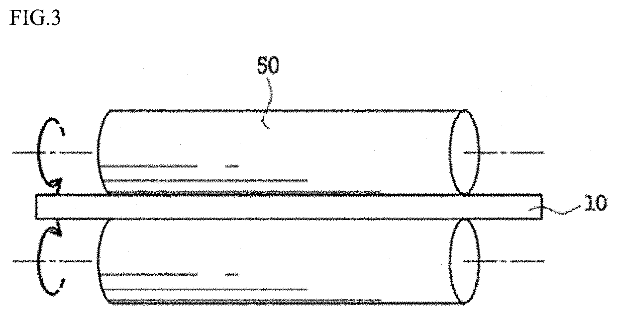
[0163]A nylon brush disposed as illustrated in FIG. 3 was equipped to the wafer manufactured in the manufacture example, and a first scrubbing operation was performed for 120 seconds by setting a rotation rate of a wafer to be 10 rpm, setting a rotation rate of a brush to be 60 rpm, and adding deionized water at 2 L / min.

[0164]A polyvinyl alcohol brush disposed as illustrated in FIG. 3 was equipped to the wafer after the first scrubbing operation, and a second scrubbing operation was performed for 90 seconds by setting a rotation rate of a wafer to be 10 rpm, setting a rotation rate of a brush to be 60 rpm, and adding an ammonia water, in which ammonia and deionized water were mixed to have a volume ratio of ammonia:deionized water of 1:20 at 2 L / min.

[0165]A polyvinyl alcohol brush disposed as illustrated in FIG. 3 was equipped to the wafer after the second scrubbing operation, and a third scrubbing operation was performed for 120 seconds by setting a rotation ...

Example

Comparative Example 1

Wafer Cleaning

[0172]Except for changing processing times of a first scrubbing operation, a second scrubbing operation, and a third scrubbing operation to be respectively 60 seconds, processing times of a first cleaning process and a second cleaning process to be respectively 150 seconds, and a processing time of a second cleaning operation to be 150 seconds from the Example 1, Comparative Example 1 was performed as same as the Example 1.

Example

Comparative Example 2

Wafer Cleaning

[0173]Except for changing processing times of a first scrubbing operation, a second scrubbing operation, and a third scrubbing operation to be respectively 90 seconds, 75 seconds, and 90 seconds, processing times of a first cleaning process and a second cleaning process to be respectively 200 seconds, and a processing time of a second cleaning operation to be 200 seconds from the Example 1, Comparative Example 2 was performed as the same as the Example 1.

[0174]

[0175]The result of ICP-MD (Inductively Coupled Plasma Mass Spectrometer, Agilent 7900) and the result of T-XRF (X-Ray Fluorescence Spectrometer, Rigaku) for wafers of the Example and Comparative Examples were shown in Table 1 and Table 2.

TABLE 1Detecting ComparativeComparativeICP-MSLimitExample 1Example 1Example 2Al1—K111—Ca1040—V0.01—Cr0.1—Mn0.159.9—Fe1—Co0.01—Ni0.10.4—Cu1—Zn1040—unit: ppb

TABLE 2ComparativeComparativeT-XRFExample 1Example 1Example 2Al—K—Ca—15.310.3V—Cr—Mn—19.6Fe—0.20.3Co—Ni...


PUM


Abstract

A method of cleaning a wafer comprises: a scrubbing operation comprising treating a target wafer to be cleaned with a brush at a rotation rate of 200 rpm or less to prepare a brush cleaned wafer; and a cleaning operation comprising cleaning the brush cleaned wafer with a cleaning solution to prepare a cleaned bare wafer, wherein the cleaning operation comprises a first cleaning operation and a second cleaning operation sequentially.

Description

CROSS-REFERENCE TO RELATED APPLICATIONS[0001]This application claims the benefit under 35 U.S.C. 119(a) of Korean Patent Application No. 10-2020-0122141 filed on Sep. 22, 2020 in the Korean Intellectual Property Office, the entire disclosure of which is incorporated herein by reference for all purposes.BACKGROUND1. Field[0002]The present disclosure relates to a method of cleaning a wafer and a wafer with reduced impurities.2. Description of the Background[0003]Silicon carbide (SiC) has excellent heat resistance and mechanical strength, and is physically and chemically stable, so that it is attracting attention as a semiconductor material. Recently, as a substrate for high power devices, the demand of silicon carbide single crystal substrates is increasing.[0004]A Chemical Mechanical Polishing (CMP) operation proceeds in manufacturing processes for a substrate (wafer) including such a silicon carbide. CMP polishes a wafer surface through rubbing the wafer with a polishing pad, and at...

Claims


Application Information

Patent Timeline
IPC IPC(8): H01L21/67H01L21/02H01L21/04B08B1/04
CPCH01L21/67046H01L21/02057B08B1/007B08B1/04H01L21/0445H01L21/02052H01L21/02068H01L21/0206H01L21/67028H01L21/67051B08B1/002B08B3/12B08B3/02H01L29/7802H01L21/02167H01L29/1608H01L29/7813C30B29/36
Inventor PARK, JONG HWIYOO, IL HWANKU, KAP-RYEOLKIM, JUNG-GYUCHOI, JUNG WOOYANG, EUN SUJANG, BYUNG KYUKO, SANG KI
Owner SENIC INC
Why Eureka
Try Eureka