
Method and system for forming silicon nitride on a sidewall of a feature

a technology of silicon nitride and sidewall, which is applied in the direction of semiconductor devices, chemical vapor deposition coatings, coatings, etc., can solve the problems of device performance, unwanted variation of silicon nitride material remaining on vertical surfaces, blistering and/or delamination of silicon nitride layer, etc., to achieve less variation of silicon nitride, less blistering and/or delamination, and better and more predictable device performance

Pending Publication Date: 2022-04-07
ASM IP HLDG BV
View PDF0 Cites 0 Cited by
  • Summary
  • Abstract
  • Description
  • Claims
  • Application Information

AI Technical Summary

Benefits of technology

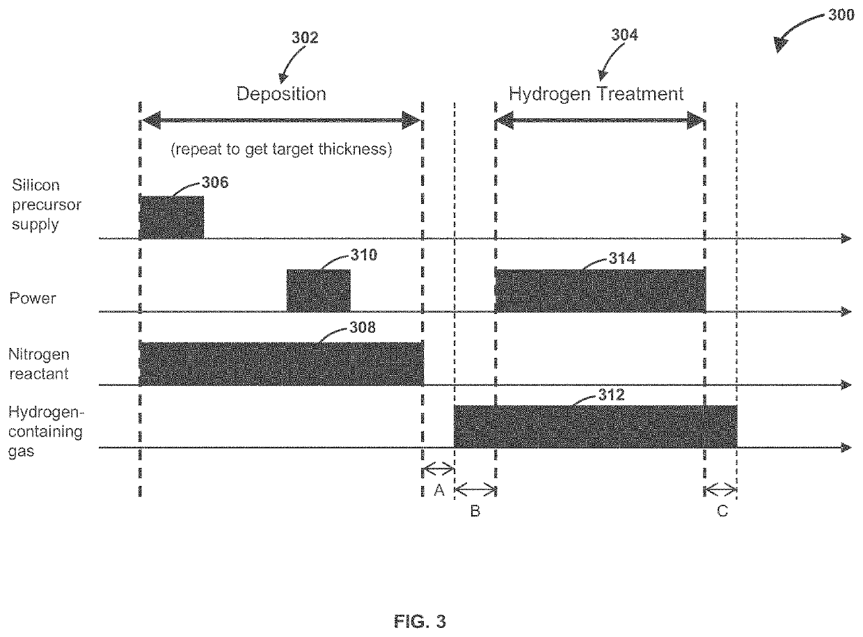
This disclosure describes improved methods of forming silicon nitride on vertical surfaces, which can result in less blistering and delamination of silicon nitride and better performance of the device. The methods can involve using plasma enhanced atomic layer deposition (PEALD) to form silicon nitride films on sidewall surfaces. This method can also result in less variation of silicon nitride formed on sidewall surfaces, which can lead to better and more predictable device performance.

Problems solved by technology

This technique can result in blistering and / or delamination of the silicon nitride layer, particularly on surfaces adjacent the sidewall surface, after treatment and before selectively removing portions of the silicon nitride layer.
The blistering and / or delamination can cause unwanted removal and / or removal variation of the silicon nitride material from or near the bottom of the vertical sidewall surfaces.
The unwanted removal of the silicon nitride material can, in turn, lead to unwanted variation in the silicon nitride material remaining on vertical surfaces and / or device performance.
The delamination and blistering can become increasingly problematic as a thickness of the silicon nitride layer decreases (e.g., to less than 20 nm or less than 10 nm).
However, such techniques often result in undesirably high amounts of the silicon nitride layer being removed near the intersection of the sidewall and the adjacent surface(s).

Method used


Image

  • Method and system for forming silicon nitride on a sidewall of a feature
  • Method and system for forming silicon nitride on a sidewall of a feature
  • Method and system for forming silicon nitride on a sidewall of a feature

Examples


Embodiment Construction

[0023]Although certain embodiments and examples are disclosed below, it will be understood by those in the art that the invention extends beyond the specifically disclosed embodiments and / or uses of the invention and obvious modifications and equivalents thereof. Thus, it is intended that the scope of the invention disclosed should not be limited by the particular disclosed embodiments described below.

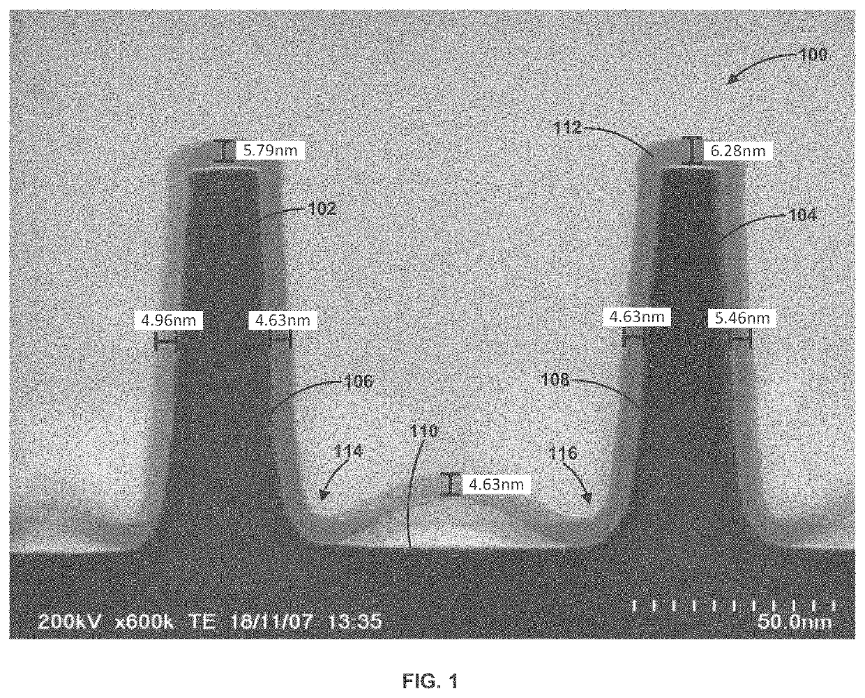
[0024]The present disclosure generally relates to methods of forming silicon nitride on a sidewall of a feature, to structures including a silicon nitride layer, and to systems for performing the methods and / or forming the structures. As described in more detail below, various methods can be used to form structures including silicon nitride on a sidewall surface of a feature, with desired silicon nitride remaining at the bottom of the sidewall / feature. Additionally or alternatively, silicon nitride on the sidewall surface can be formed in a more predictable manner and / or device perform...


PUM

PropertyMeasurementUnit
thicknessaaaaaaaaaa
thicknessaaaaaaaaaa
thicknessaaaaaaaaaa

Abstract

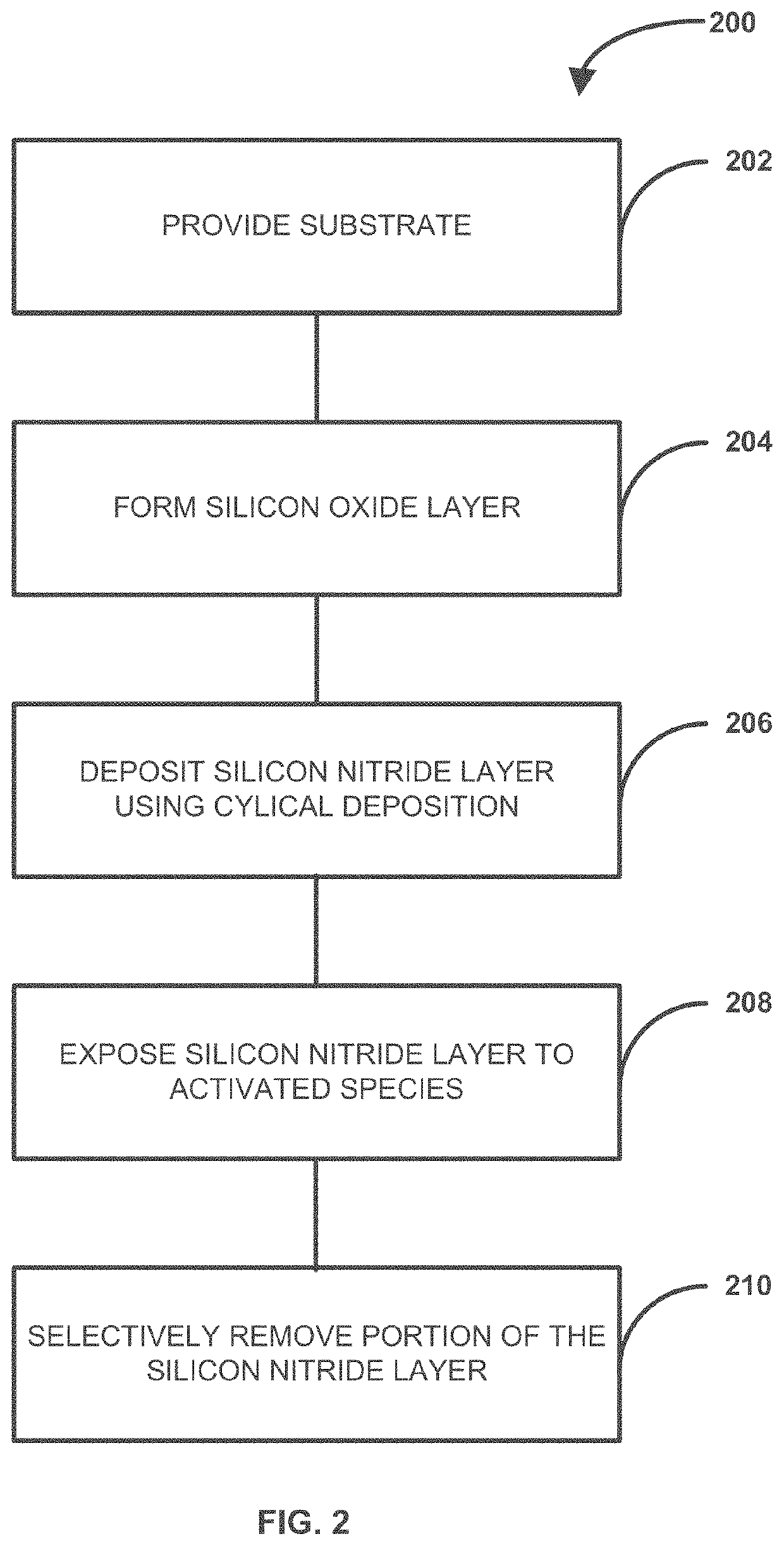
Methods of forming silicon nitride on a sidewall of a feature are disclosed. Exemplary methods include providing a substrate comprising a feature comprising a sidewall surface and a surface adjacent the sidewall surface, forming a silicon oxide layer overlying the sidewall surface and the surface adjacent the sidewall surface, using a cyclical deposition process, depositing a silicon nitride layer overlying the silicon oxide layer, and exposing the silicon nitride layer to activated species generated from a hydrogen-containing gas. Exemplary methods can additionally include selectively removing a portion of the silicon nitride layer. Structures formed using the methods and systems for performing the methods are also disclosed.

Description

CROSS-REFERENCE TO RELATED APPLICATIONS[0001]This application claims priority to U.S. Application No. 63 / 088,078, filed on Oct. 6, 2020 in the United States Patent and Trademark Office, the disclosure of which is incorporated herein in its entirety by reference.FIELD OF INVENTION[0002]The present disclosure generally relates to methods and systems for forming devices. More particularly, examples of the disclosure relate to methods and systems for forming silicon nitride on surfaces of a substrate.BACKGROUND OF THE DISCLOSURE[0003]Silicon nitride layers can be used for a variety of applications during the formation of electronic devices. For example, silicon nitride layers can be used as dielectric layers, diffusion barriers, hard masks, spacers, and the like.[0004]In some applications, it may be desirable to form silicon nitride primarily on sidewall surfaces of features, such that no or relatively little silicon nitride remains on surfaces adjacent the sidewalls (e.g., top and bott...

Claims


Application Information

Patent Timeline
Patent Type & Authority Applications(United States)
IPC IPC(8): H01L21/02H01L21/311
CPCH01L21/0217H01L21/02164H01L21/0228H01L21/0234H01L21/02274H01L21/31111H01L21/31116H01L21/02211C23C16/345C23C16/455H01L21/76237H01L21/02H01L21/02304H01L21/0337H01L29/66795C23C16/045C23C16/401C23C16/45523C23C16/56C23C16/505H01L21/02219
Inventor KUBOTA, TOMOHIROUEDA, SHINYA
Owner ASM IP HLDG BV
Learn More