Stress-reduced circuit board and method for forming the same
a circuit board and stress reduction technology, applied in the field of circuit boards, can solve the problems of complex manufacturing process, low availability of materials for making the same, and increased production costs, so as to achieve less likely to suffer delamination, cracking and warpage.
Active Publication Date: 2016-10-11
TONG HSING ELECTRONICS IND LTD
View PDF9 Cites 0 Cited by
- Summary
- Abstract
- Description
- Claims
- Application Information
AI Technical Summary
Benefits of technology
The present invention provides a circuit board that is less likely to have delamination, cracking, and warping due to temperature variations. This circuit board can be produced on a large scale for use in high-power electronic devices. Additionally, this patent describes a method for forming this circuit board. The technical effect of this invention is to improve the reliability and efficiency of circuit boards used in electronic devices.
Problems solved by technology
However, since there is a serious “CTE mismatch” between a ceramic material (Al2O3: 6.9 mm / m° C.) and a copper material (16.4 mm / m° C
.), and since the circuits are made from a relatively thick copper layer, after a period of use of the high-power electronic device, undesirable cracking and warpage of the ceramic substrate, and delamination of the circuits from the ceramic substrate may result.
However, the aforesaid conventional composite substrates / circuit boards are disadvantageous in that the materials for making the same may not be readily accessible and the manufacturing process involved is complicated.
In addition, they are likely to suffer delamination, cracking and warpage in response to temperature variation due to hetero-junctions between multiple layers thereof.
Method used
View moreImage
Smart ImageViewing Examples
Examples
example 1
[0081]A circuit board 1 of Example 1 was formed according to the first embodiment of the method for forming the circuit board 1 in the first preferred embodiment, and has a structure shown in FIG. 31. The circuit board 1 has the electrically conductive unit 4 on the upper side thereof, and a copper layer 44 which fully covers a lower surface of the insulating substrate 2, and which has a thickness of 80˜90 μm. The electrically conductive unit 4 and the seed layer 3 together have a height of about 180 μm. The electrically conductive unit 4 was made from a copper material, and the insulating substrate 2 was made from a ceramic material.
Login to View More PUM
 Abstract
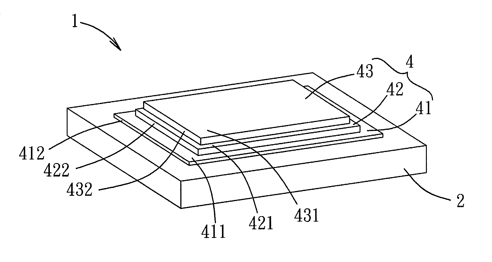
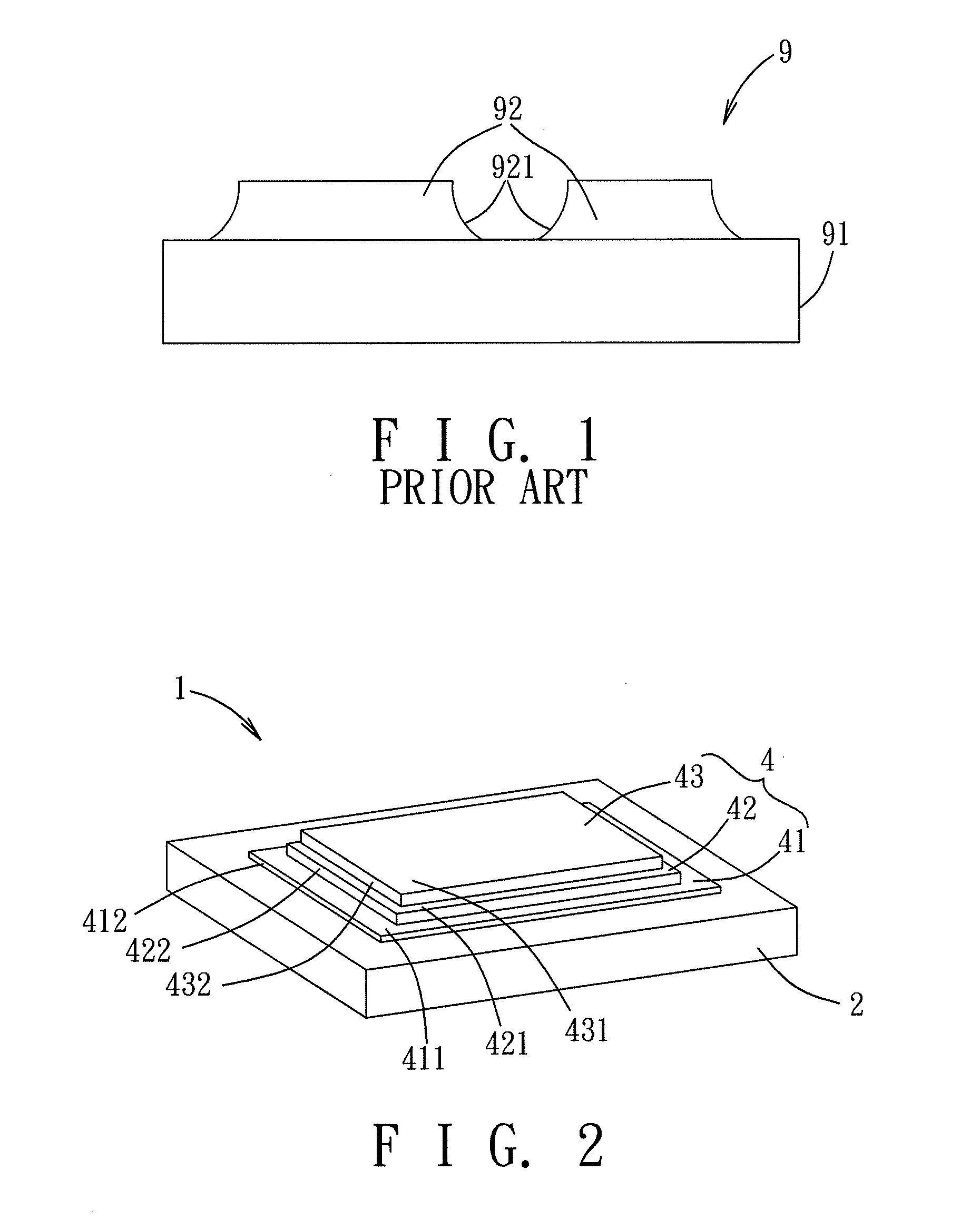
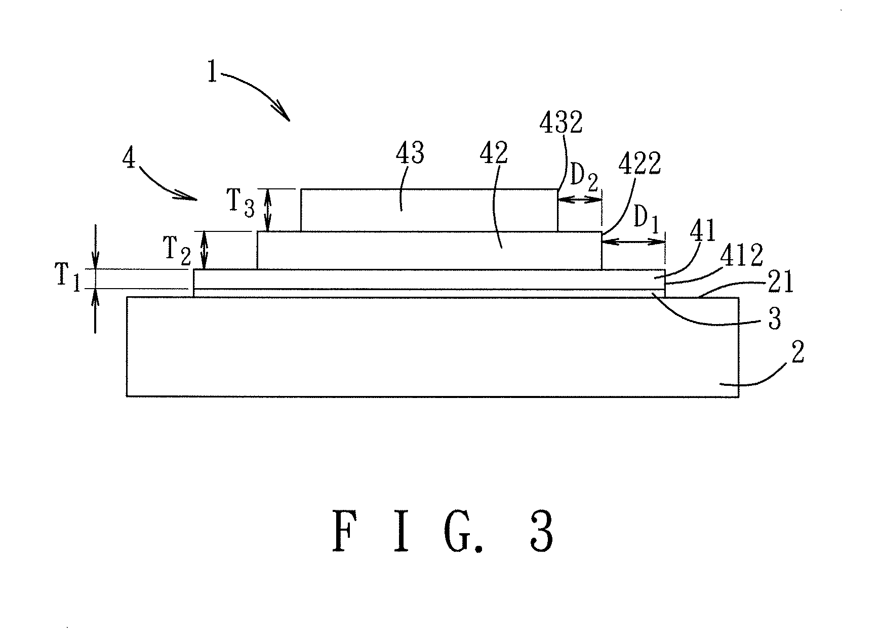
A stress-reduced circuit board includes an insulating substrate, and first and second electrically conductive layers which are stacked one upon the other, and which respectively have peripheral marginal regions that are configured in a stepped arrangement. The first electrically conductive layer is configured to have an area dimension larger than that of the second electrically conductive layer and a thickness not greater than that of the second electrically conductive layer so as to minimize stress caused by a difference in coefficients of thermal expansion between the insulating substrate and the first and second electrically conductive layers.
Description
CROSS-REFERENCE TO RELATED APPLICATION[0001]This application claims priority of Taiwanese application no. 101138461, filed on Oct. 18, 2012.BACKGROUND OF THE INVENTION[0002]1. Field of the Invention[0003]This invention relates to a circuit board, more particularly to a stress-reduced circuit board and a method for forming the same.[0004]2. Description of the Related Art[0005]A ceramic substrate, which has a relatively high thermal conductivity, a relatively low coefficient of thermal expansion (CTE), and excellent properties of heat-resistance and chemical-resistance, is generally used in a direct bonded copper (DBC) substrate for high heat dissipation and high-efficiency electronic devices, such as insulated-gate bipolar transistors (IGBTs), thermal electrical coolers / generators (TECs / TEGs), light-emitting diodes (LEDs), etc. In general, such a DBC substrate is made by high-temperature eutectic-bonding a copper foil to a fired ceramic substrate, and patterning a copper layer of the...
Claims
Login to View More Application Information
Patent Timeline
 Patent Type & Authority Patents(United States)
IPC IPC(8): H05K1/02H05K3/06H05K3/00H05K1/03H05K3/10H05K3/14H05K3/16H05K3/38
CPCH05K1/0271H05K1/0265H05K2201/09845H05K2203/058H05K2203/1476H05K2203/1572H05K1/0306H05K3/06H05K3/108H05K3/146H05K3/16H05K3/388H05K2201/0338
Inventor WEI, CHIEN-CHENGCHENG, WU-HUI
Owner TONG HSING ELECTRONICS IND LTD


