Display panel and method of manufacturing the same

a display panel and manufacturing method technology, applied in the direction of transistors, electrical devices, semiconductor devices, etc., can solve the problems of low carrier mobility, failure to meet the high-definition picture quality requirements of the next-generation oled display device, and complex structure of the top gate igzo tft of the related art, so as to reduce the number of oxide tft layers, simplify the film structure of the display panel, and reduce the process and mask requirements

Pending Publication Date: 2022-04-14
SHENZHEN CHINA STAR OPTOELECTRONICS SEMICON DISPLAY TECH CO LTD
View PDF0 Cites 0 Cited by
  • Summary
  • Abstract
  • Description
  • Claims
  • Application Information

AI Technical Summary

Benefits of technology

The present patent proposes a display panel and manufacturing method that solves issues of complicated structure and high cost associated with conventional display panels. The panel features a source / drain layer and light shielding layer on the same layer of the substrate, which helps reduce the number of oxide TFT layers, simplifying the film structure, reducing processes and masks required for production, and increasing production efficiency and reducing costs.

Problems solved by technology

A hydrogenated amorphous silicon (a-Si:H) TFT is the most widely applied TFT technology, but limited by low carrier mobility.
The technology fails to meet the high-definition picture quality requirements of a next-generation OLED display device.
The structure of a TOP Gate IGZO TFT of the related art is complicated, which requires eight or more lithography processes to produce a light shielding layer to the pixel electrode layer.
Due to two many masks and production processes required, resulting in high production costs, it is hard to manufacture the TOP Gate IGZO TFT.
In sum, the structure of the oxide film TFT of the related art is complicated with too many manufacturing processes, resulting on high production cost.
The display panel and the display panel are configured to solve problems of the related art such as an oxide film thin film transistor (TFT) of a complicated structure, too many manufacturing processes, and high production cost.

Method used


Image

  • Display panel and method of manufacturing the same
  • Display panel and method of manufacturing the same
  • Display panel and method of manufacturing the same

Examples


embodiment 1

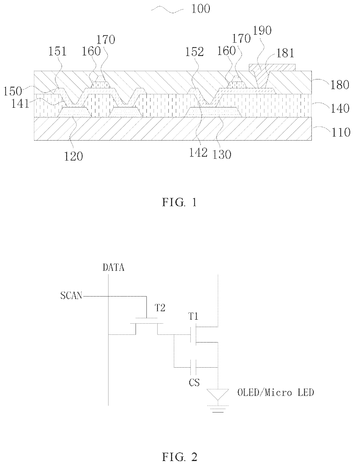
[0028]A first embodiment of the present disclosure provides a display panel, which will be described in detail below with reference to FIG. 1 and FIG. 2.

[0029]FIG. 1 is a schematic diagram of a display panel 100 from a cross-sectional view according to the first embodiment of the disclosure. The display panel 100 includes a substrate 110, a source / drain layer 120, a light shielding layer 130, a dielectric layer 140, and an oxide semiconductor layer 150.

[0030]In the present embodiment, the source / drain layer 120 is disposed on the substrate 110. The light shielding layer 130 is disposed on the substrate 110. The light shielding layer 130 and the source / drain layer 120 is disposed on the same layer. The dielectric layer 140 is disposed on the substrate 110 and covers the light shielding layer 130 and the source / drain layer 120. The first hole 141 and the second hole 142 are disposed on the dielectric layer 140. The first hole 141 and the second hole 142 expose the source / drain layer 1...

embodiment 2

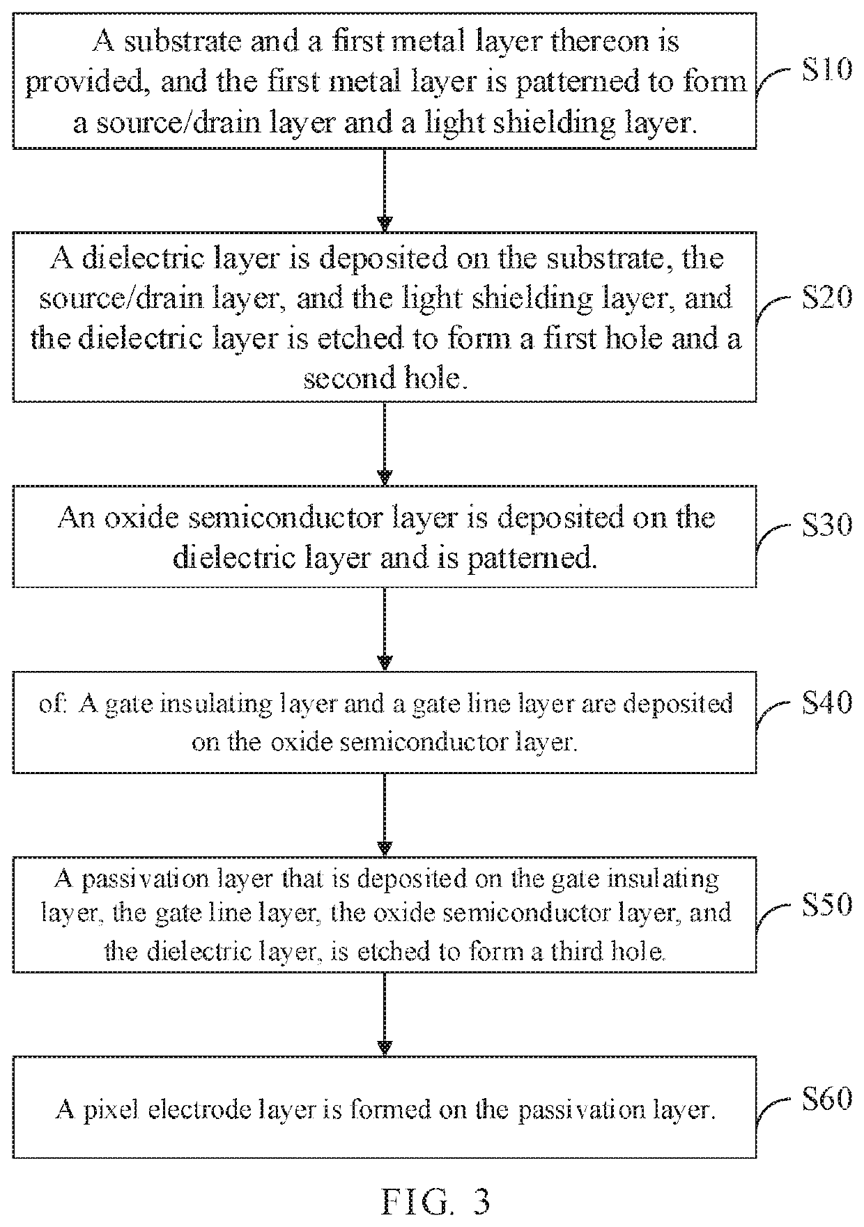
[0048]A second embodiment of the present disclosure further proposes a method of manufacturing a display panel 200. The manufacturing method will be described in detail below with reference to FIG. 3 to FIG. 9. The manufacturing method includes a block S10, a block S20, a block S30, a block S40, a block S50, and a block S60.

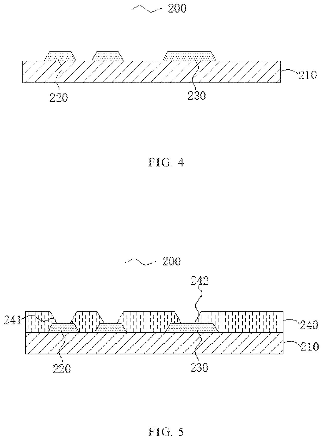
[0049]At block S10, as illustrated in FIG. 4, a substrate 210 is provided. A first metal layer is deposited on the substrate 210. The first metal layer is patterned to form a source / drain layer 220 and a light shielding layer 230.

[0050]The first metal layer is of a stacked structure of molybdenum and copper or a stacked structure of aluminum and molybdenum in the second embodiment.

[0051]At block S20, as illustrated in FIG. 5, a dielectric layer 240 is deposited on the substrate 210, the source / drain layer 220, and the light shielding layer 230. The dielectric layer 240 is etched to form a first hole 241 and a second hole 242.

[0052]In another embodiment, material ...


PUM

PropertyMeasurementUnit
semiconductoraaaaaaaaaa
dielectricaaaaaaaaaa
insulatingaaaaaaaaaa

Abstract

A display panel and a manufacturing method are provided. The display panel includes a substrate, a source / drain layer, a light shielding layer, a dielectric layer disposed on the substrate and covering the light shielding layer and the source / drain layer, and an oxide semiconductor layer disposed on the dielectric layer. The oxide semiconductor layer is connected to the source / drain layer and the light shielding layer through a first hole and a second hole, respectively. A metal layer is etched to form the source / drain layer and the light shielding layer simultaneously. The dielectric layer arranged on the substrate covers the light shielding layer and the source / drain layer. The dielectric layer functions as an isolating layer, which reduces the number of oxide TFT layers of the display panel, simplifying the film structure of the display panel, reducing the processes and masks required for production, thereby increasing production efficiency and reducing production costs.

Description

BACKGROUND1. Field of the Disclosure[0001]The present disclosure relates to the field of manufacturing a display panel, and more particularly, to a display panel and a method of manufacturing the display panel.2. Description of the Related Art[0002]The display device industry, as an electronic information industry with development potential, has developed rapidly in recent years. The mainstream organic light-emitting diode (OLED) display device industry has become one of the pillar industries in the electronic information industry. A thin film transistor (TFT) is a core device of a flat panel display. A TFT is usually configured as an address switching device in an OLED display device. A hydrogenated amorphous silicon (a-Si:H) TFT is the most widely applied TFT technology, but limited by low carrier mobility. The technology fails to meet the high-definition picture quality requirements of a next-generation OLED display device. The TFT plays a vital role in an OLED display pixel circ...

Claims


Application Information

Patent Timeline
Patent Type & Authority Applications(United States)
IPC IPC(8): H01L27/12H01L29/786H01L21/02H01L29/66
CPCH01L27/1225H01L27/127H01L29/66969H01L29/7869H01L21/02565H01L29/78633H01L27/1259H10K59/1213
Inventor LU, MACAI
Owner SHENZHEN CHINA STAR OPTOELECTRONICS SEMICON DISPLAY TECH CO LTD
Why Eureka
Try Eureka