
Semiconductor module, semiconductor member, and method for manufacturing the same

Pending Publication Date: 2022-05-05
ULSTREETCAREMORY INC
View PDF0 Cites 1 Cited by
  • Summary
  • Abstract
  • Description
  • Claims
  • Application Information

AI Technical Summary

Benefits of technology

The present invention is about a semiconductor module and member that can improve heat dissipation. The invention also provides a method for manufacturing these semiconductor components. The technical effect of the invention is to enhance the heat dissipation efficiency of semiconductor modules and members.

Problems solved by technology

On the other hand, this type of increase in capacity is reaching its limit because of the miniaturization resulting in feebleness to noise, an increase in die area, and other factors.

Method used


Image

  • Semiconductor module, semiconductor member, and method for manufacturing the same
  • Semiconductor module, semiconductor member, and method for manufacturing the same
  • Semiconductor module, semiconductor member, and method for manufacturing the same

Examples


first embodiment

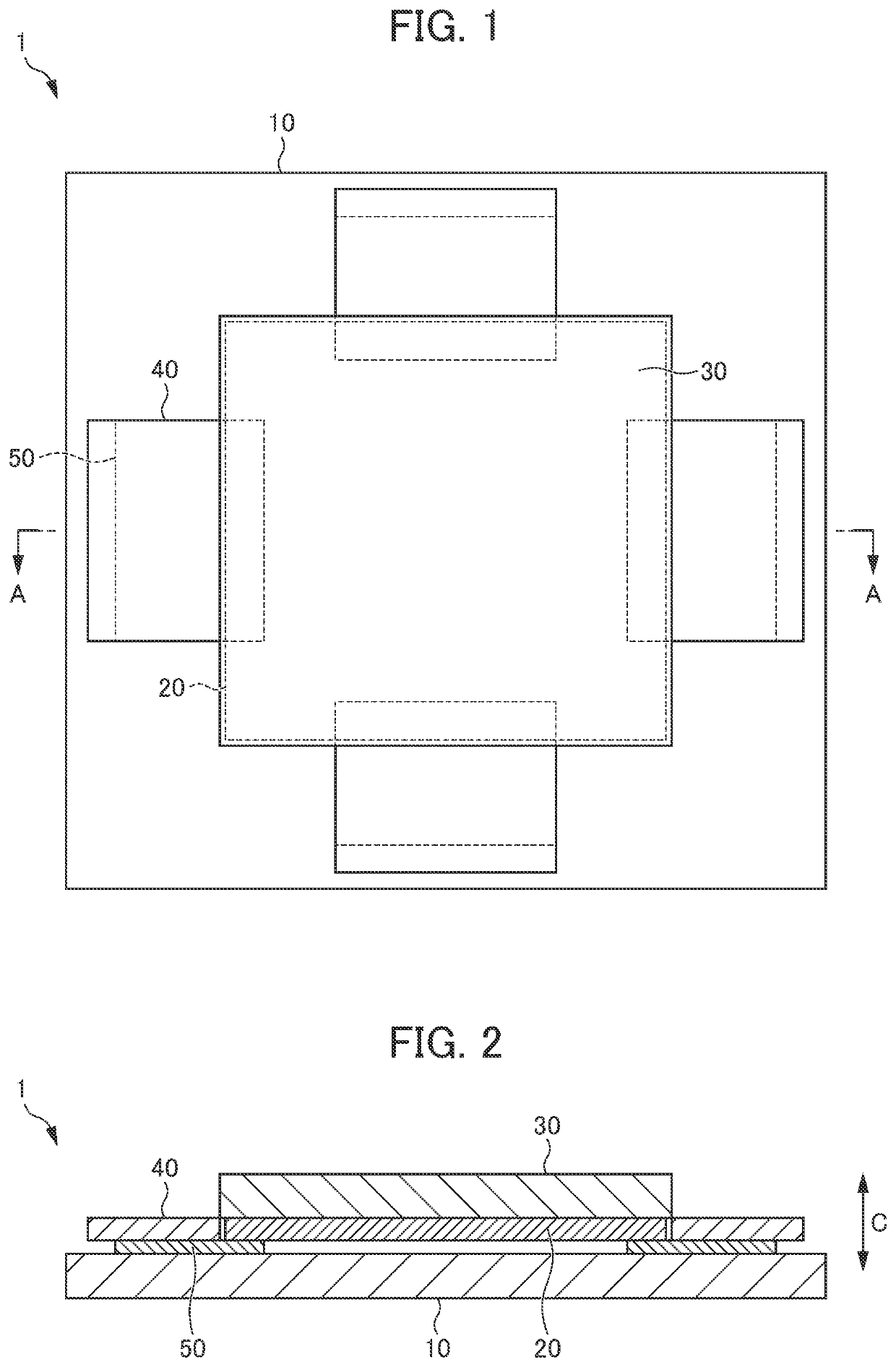
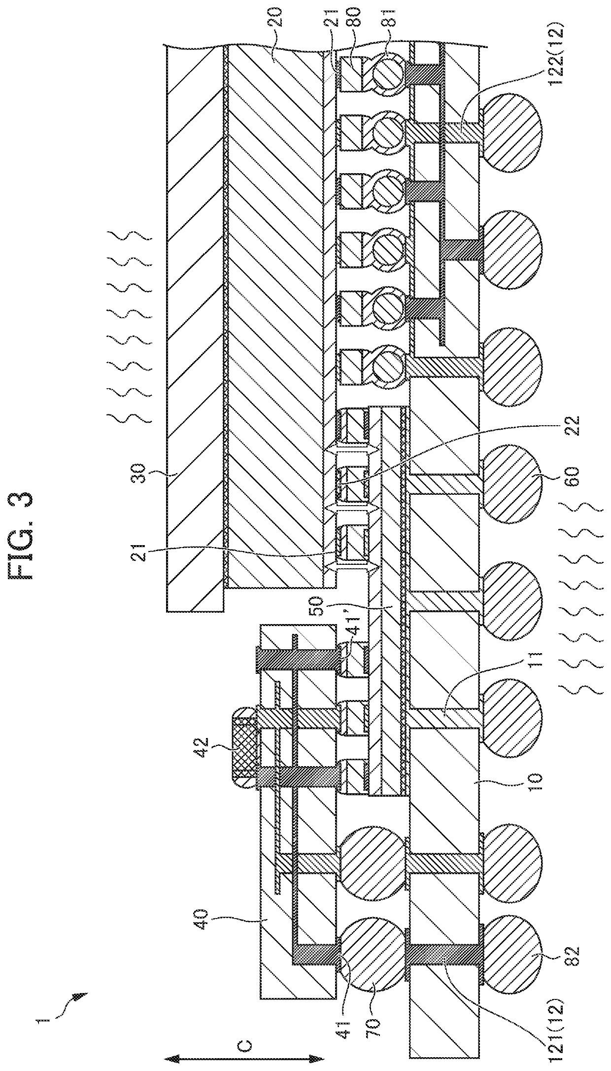
[0038]Next, a semiconductor module 1 according to a first embodiment and a method for manufacturing the semiconductor module 1 will be described with reference to FIGS. 1 to 9. As illustrated in FIGS. 1 to 3, the semiconductor module 1 according to the first embodiment includes a heat spreader 30, a MPU 20, a power supply unit 40, a RAM unit 50, a support substrate 10, and a heat dissipation ball 60. In the semiconductor module 1 of the present embodiment, the MPU 20 includes one MPU 20, the RAM unit 50 includes four RAM units 50, and the power supply unit 40 includes four power supply units 40. These components are all disposed over the support substrate 10 including one support substrate 10.

[0039]The heat spreader 30 is made of, for example, a material having relatively high heat dissipation efficiency, such as a metal. In the present embodiment, the heat spreader 30 has a rectangular plate shape in planar view, as illustrated in FIGS. 1 to 3. The heat spreader 30 may have, for ex...

second embodiment

[0057]Next, a semiconductor module 1 and a semiconductor member 100 according to a second embodiment of the present invention, and a method for manufacturing the semiconductor module and member will be described with reference to FIGS. 10 to 17. In the description of the second embodiment, the same components as those of the above-described embodiment will be denoted by the same reference characters, and a description of the same components will be omitted or simplified. As illustrated in FIGS. 10 to 12, the semiconductor module 1 according to the second embodiment differs from that of the first embodiment in that in the second embodiment, a heat spreader 30 is adjacent to power supply units 40 in a thickness direction C. Further, the semiconductor module 1 according to the second embodiment differs from that of the first embodiment in that each power supply unit 40 of the second embodiment is configured as a power supply die including therein, for example, a power supply circuit (n...

third embodiment

[0067]Next, a semiconductor module 1 according to a third embodiment of the present invention and a method for manufacturing the semiconductor module 1 will be described with reference to FIGS. 18 and 19. In the description of the third embodiment, the same components as those of the above-described embodiments will be denoted by the same reference characters, and a description of the same components will be omitted or simplified. As illustrated in FIGS. 18 and 19, the semiconductor module 1 according to the third embodiment differs from that of the second embodiment in that a support substrate 10 of the third embodiment has, on one main surface, recesses 13 that are recessed in a thickness direction C and are formed at positions over which RAM units 50 are superimposed.

[0068]Each recess 13 has a depth that enables connection to the MPU 20 and the power supply unit 40 only by means of Cu pillars 80 and solder bumps 71 provided on one main surface of the support substrate 10, without...


PUM


Abstract

The present invention provides a semiconductor module, a semiconductor member, and a method for manufacturing the same that make it possible to improve heat dissipation efficiency. This semiconductor module 1 comprises: a power supply unit 40; a RAM unit 50, which is a RAM module having a facing surface disposed so as to face an exposed surface of a logic chip 20 and an exposed surface of the power supply unit 40, the RAM module being disposed across some of a plurality of logic chip signal terminals 22 and some of a plurality of power supply unit power supply terminals 41; and a support substrate 10 having a power feeding circuit capable of feeding electrical power to the logic chip and to the power supply unit 40, one main surface of the support substrate 10 being disposed adjacent to a heat dissipation surface of the RAM unit 50, which is the surface of the RAM unit 50 opposite the facing surface. The support substrate 10 is electrically connected, using the power feeding circuit 12, to at least some of logic chip power supply terminals 21 and the other power supply unit power supply terminals 41. The support substrate 10 has, at positions overlapping the RAM unit 50, heat dissipation vias 11 that penetrate in the thickness direction and come into contact with the heat dissipation surface of the RAM unit 50.

Description

TECHNICAL FIELD[0001]The present invention relates to a semiconductor module, a semiconductor member, and a method for manufacturing the same.BACKGROUND ART[0002]A volatile memory (RAM), such as a dynamic random access memory (DRAM), has been known as a storage device. The DRAM is required to have a large capacity such that it can support high performance of an arithmetic unit (hereinafter referred to as a logic chip) and an increase in an amount of data. To address this, the capacity has been increased by miniaturization of the memory (memory cell array, memory chip) and planar expansion of a cell. On the other hand, this type of increase in capacity is reaching its limit because of the miniaturization resulting in feebleness to noise, an increase in die area, and other factors.[0003]Therefore, in recent years, a technique for achieving a large capacity by way of a three-dimensional (3D) structure that is formed by stacking a plurality of planar memories has been developed. Further...

Claims


Application Information

Patent Timeline
IPC IPC(8): G11C11/4074H01L27/108H01L25/00
CPCG11C11/4074H01L25/50H01L27/10847H01L27/10805H01L25/18H01L23/36G11C5/04G11C7/04H01L2224/73253H01L2225/06513H01L2225/06517H01L2225/06589H01L2225/06555H01L23/49816H01L23/5384H01L23/50H10B12/50H10B12/02H10B12/30G11C5/14G11C11/4063
Inventor OKUTSU, FUMITAKEADACHI, TAKAO
Owner ULSTREETCAREMORY INC
Learn More