
Systems, devices, and methods for resistance metrology using graphene with superconducting components

a superconductor and graphene technology, applied in the field of resistance metrology, can solve the problems of accumulated internal resistance, unwelcome hall resistance contributions, slow electrical properties, etc., and achieve the effects of improving contact geometries, improving resistance standards, and prolonging the life of quantum hall resistance apparatuses

Pending Publication Date: 2022-05-12
US REPRESENTED BY SEC OF COMMERCE
View PDF5 Cites 2 Cited by
  • Summary
  • Abstract
  • Description
  • Claims
  • Application Information

AI Technical Summary

Benefits of technology

This patent relates to improving resistance metrology systems by tailoring equivalent values to meet different needs. The invention uses multiple Hall bar elements that do not have accumulated internal resistances due to contacts and resistive metallic interconnections. The system also uses superconducting connections and improved contact geometries. Additionally, this patent proposes chemically functionalizing graphene to extend the life of quantum Hall resistance apparatuses.

Problems solved by technology

One issue for these scalable resistance networks, based on multiple Hall bar elements, is that they suffer from accumulated internal resistances directly from contacts, spreading, and wires, and unwanted Hall resistance contributions from resistive metallic interconnections.
Further, even though the graphene has shown superior properties for the development of quantum Hall resistance (QHR) standards, one major difficulty with a QHR device based on the graphene is that their electrical properties drift slowly over time if the QHR device is stored in air due to adsorption of atmospheric molecular dopants.

Method used


Image

  • Systems, devices, and methods for resistance metrology using graphene with superconducting components
  • Systems, devices, and methods for resistance metrology using graphene with superconducting components
  • Systems, devices, and methods for resistance metrology using graphene with superconducting components

Examples


Embodiment Construction

[0043]The present disclosure relates to systems and methods for making a quantum Hall resistance device for resistance metrology. The quantum Hall resistance device includes a network of Hall bar elements, which can be configured to make a resistance standard, which can be used for resistance metrology. The Hall bar elements are made of graphene and connected to contacts, which are made of superconducting material so as to decrease resistances between the Hall bar elements and the contacts. The graphene is epitaxially grown on a substrate and shows electrically improved conductivity.

[0044]When the graphene is chemically functionalized, the carrier density may be controlled or stabilized under ambient conditions, thereby enlarging the life of the quantum Hall resistance devices.

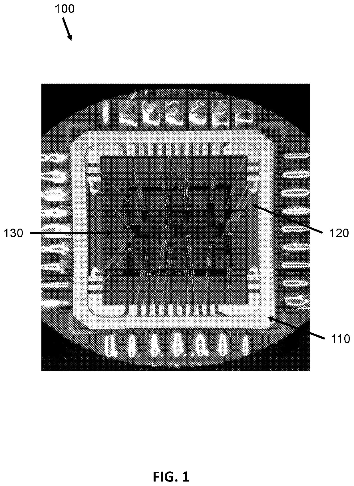
[0045]FIG. 1 shows a quantum Hall resistance device 100 in accordance with aspects of the present disclosure. The illustrated quantum Hall resistance device 100 includes a leadless chip carrier 110 and an arra...


PUM


Abstract

A quantum Hall resistance apparatus is to improve resistance standards and includes a substrate, a graphene epitaxially grown on the substrate and having a plurality of first contact patterns at edges of the graphene, a plurality of contacts, each including a second contact pattern and configured to connect to a corresponding first contact pattern, and a protective layer configured to protect the graphene and to increase adherence between the first contact patterns and the second contact patterns. The contacts become a superconductor at a temperature lower than or equal to a predetermined temperature and under up to a predetermined magnetic flux density.

Description

CROSS-REFERENCE TO RELATED APPLICATION[0001]This application claims the benefit of, and priority to, U.S. Provisional Patent Application No. 62 / 813,526, filed on Mar. 4, 2019, of which entire contents are hereby incorporated by reference.GOVERNMENT SUPPORT STATEMENT[0002]This invention was made with government support under 70NANB16H168 awarded by National Institutes of Standards and Technology. The government has certain rights in the invention.BACKGROUNDTechnical Field[0003]The present disclosure relates generally to resistance metrology and, more particularly, to resistance standards using graphene with superconductor materials.Related Art[0004]Graphene was first isolated as micrometer-size exfoliated flakes from bulk graphite and found to have favorable electrical and optical properties. Scalability and homogeneity of the graphene have improved to the point that one can realize devices suitable for general applications, like larger scale electronics, and more specialized applica...

Claims


Application Information

Patent Timeline
IPC IPC(8): G01R33/00G01R33/07G01R33/035H01L39/12H01L39/04
CPCG01R33/0052G01R33/07H01L39/04H01L39/12G01R33/035G01R35/007G01R27/14H10N52/80H10N52/01H10N60/81H10N60/85
Inventor ELMQUIST, RANDOLPHRIGOSI, ALBERTKRUSKOPF, MATTIAS
Owner US REPRESENTED BY SEC OF COMMERCE
Learn More