
Semiconductor device, electric power conversion device, and manufacturing method of semiconductor device

a semiconductor device and manufacturing method technology, applied in semiconductor devices, semiconductor/solid-state device details, solid-state devices, etc., can solve the problems of power semiconductor modules to fail, defective parts concentrated electric field and corona discharge, etc., to suppress corona discharge.

Pending Publication Date: 2022-05-26
HITACHI LTD
View PDF0 Cites 0 Cited by
  • Summary
  • Abstract
  • Description
  • Claims
  • Application Information

AI Technical Summary

Benefits of technology

The invention can help prevent corona discharge from happening in a sealing member's defective part.

Problems solved by technology

A high voltage is applied to a semiconductor element in a power semiconductor module, and thus, if a defect such as a gap or a crack exists in an insulating member such as a case for accommodating the semiconductor element, there is a possibility that an electric field is concentrated in the defective part and corona discharge occurs.
If the corona discharge continues to occur, there is a risk that the insulating member deteriorates and eventually breaks down, causing the power semiconductor module to fail.

Method used


Image

  • Semiconductor device, electric power conversion device, and manufacturing method of semiconductor device
  • Semiconductor device, electric power conversion device, and manufacturing method of semiconductor device
  • Semiconductor device, electric power conversion device, and manufacturing method of semiconductor device

Examples


first embodiment

[0034]Hereinafter, a first embodiment of a semiconductor device of the present invention will be described with reference to FIG. 1 to FIG. 14.

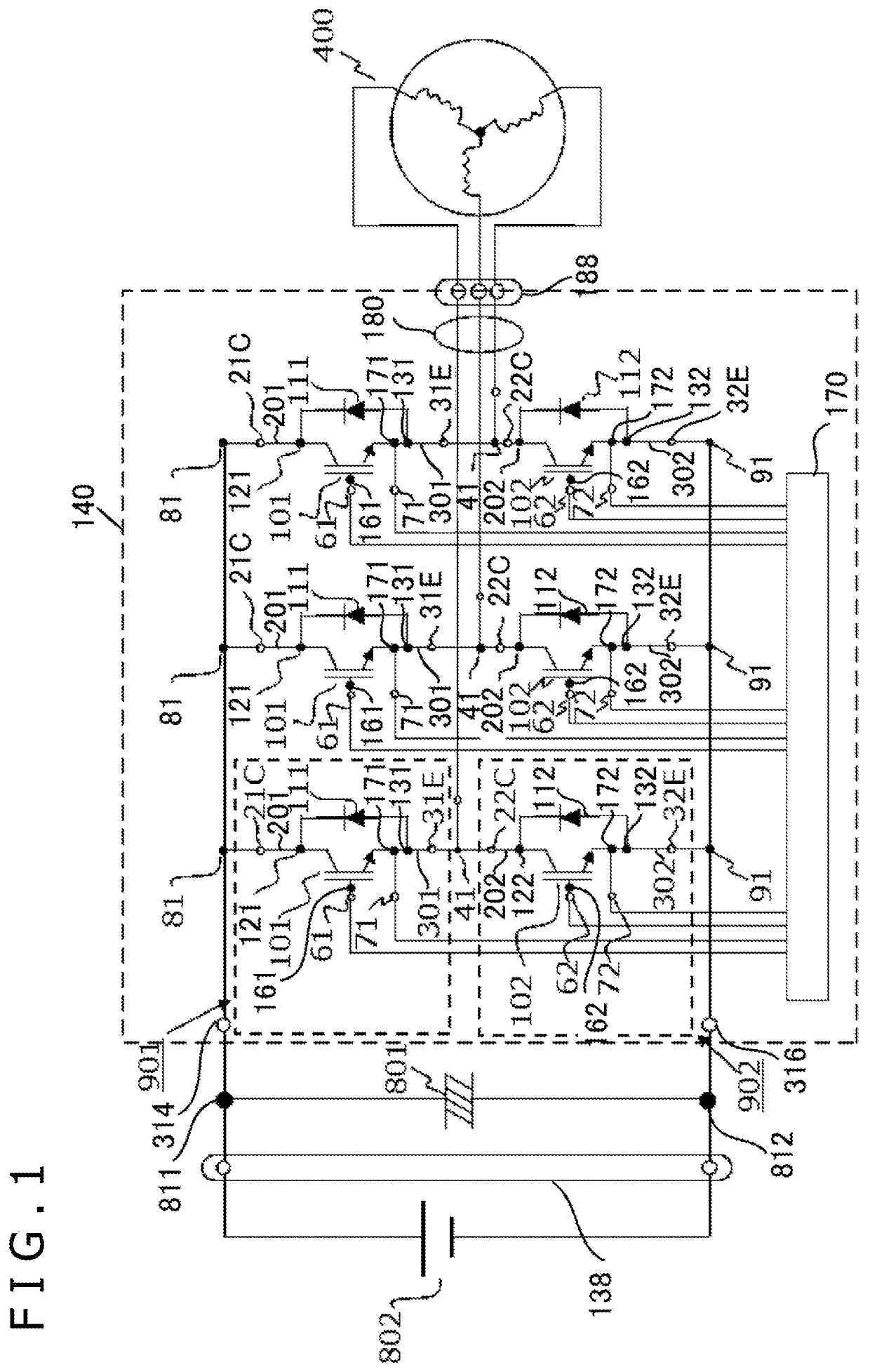
[0035]FIG. 1 is a circuit diagram of a semiconductor device having an electric power conversion circuit of the present invention.

[0036]The semiconductor device having a function as an electric power conversion device includes an inverter circuit 140, a smoothing capacitor module 801, and a control unit 170. A battery 802 is electrically connected to the inverter circuit 140. The capacitor module 801 provided between the battery 802 and the inverter circuit 140 smooths a DC current. The smoothing capacitor module 801 has a positive-side capacitor terminal 811 and a negative-side capacitor terminal 812. The smoothing capacitor module 801 is electrically connected to the battery 802 via a DC connector 138. The inverter circuit 140 is connected to the positive-side capacitor terminal 811 via a DC positive-side terminal 314, and is connected to th...

second embodiment

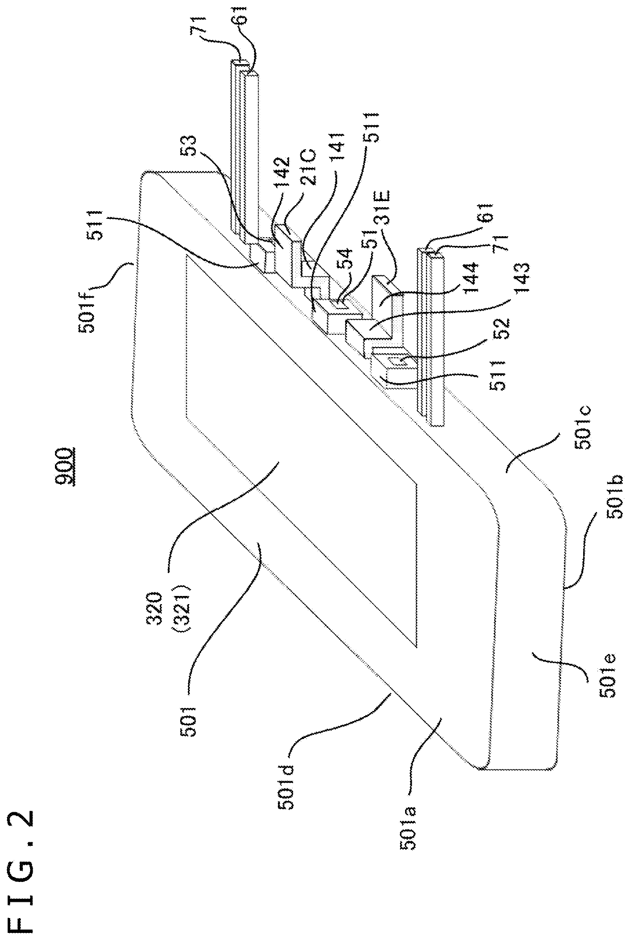
[0139]FIG. 15 is an external perspective view for showing a second embodiment of the semiconductor device of the present invention, and FIG. 16 is a plan view of the semiconductor device illustrated in FIG. 15 by seeing through an emitter-side mounting part from the upper surface side.

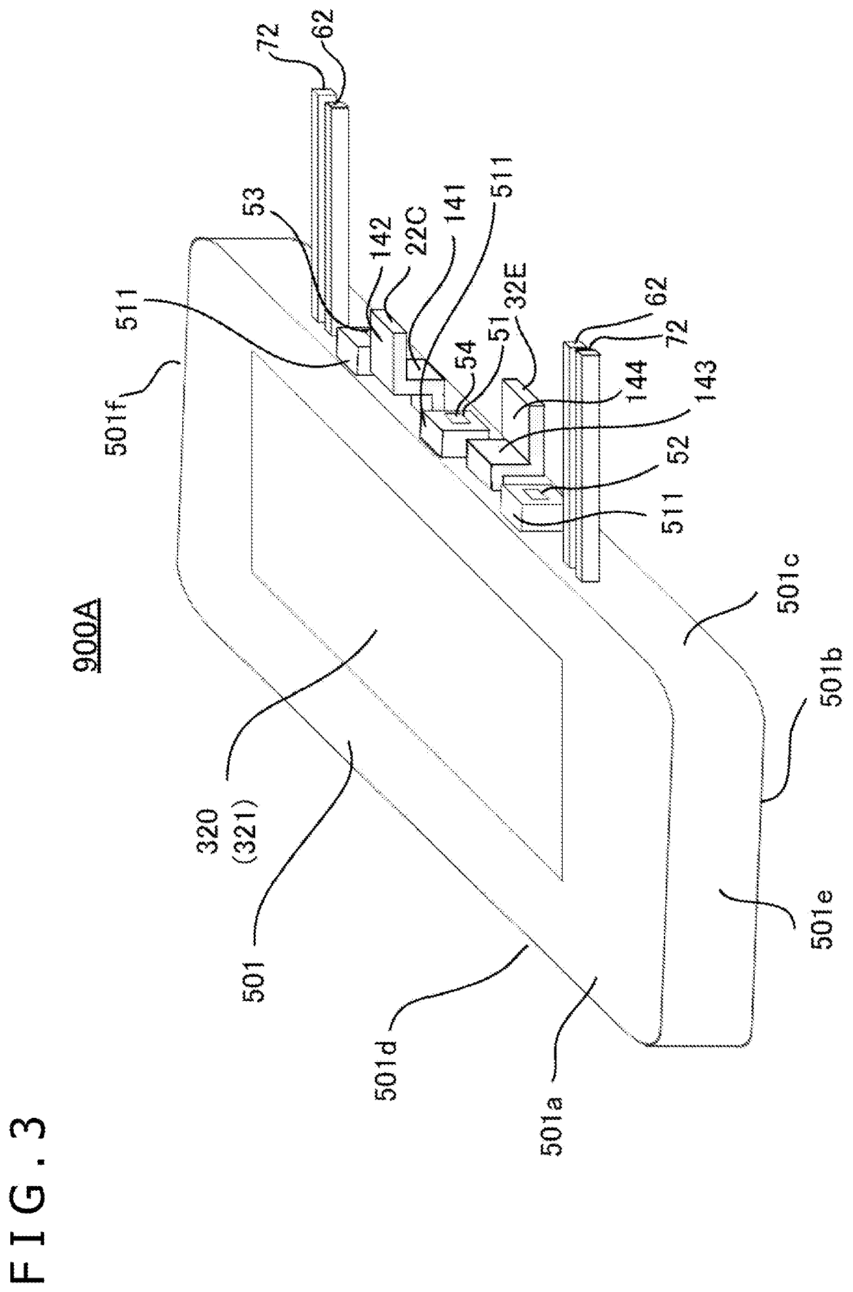
[0140]A semiconductor device 900 of the second embodiment is a 2-in-1 power semiconductor module having an upper arm circuit 901 and a lower arm circuit 902.

[0141]That is, the semiconductor device 900 of the second embodiment has IGBTs 101 and 102, diodes 111 and 112, a collector terminal 21C, an emitter terminal 32E, an emitter terminal 31E (collector terminal 22C), gate terminals 61 and 62, and emitter sense terminals 71 and 72. As illustrated in FIG. 1, the IGBT 101 has the gate electrode 161, the collector electrode 121, the emitter electrode 131, and the emitter sense electrode 171, and the IGBT 102 has the gate electrode 162, the collector electrode 122, the emitter electrode 132, and the emitter...

third embodiment

[0159]FIG. 17 shows a third embodiment of the semiconductor device of the present invention and is a plan view of the semiconductor device by seeing through an emitter-side mounting part from the upper surface side.

[0160]A semiconductor device 900 of the third embodiment is different from the first embodiment in that each tip end surface 54 of floating terminals 51, 52, and 53 is covered with a protruding part 511 of a sealing member 501. In addition, the semiconductor device 900 of the third embodiment is different from the first embodiment in that floating electrodes 530 connected to root-side end portions of the respective floating terminals 51, 52, and 53 are provided.

[0161]Other structures are the same as those in the first embodiment.

[0162]In the semiconductor device 900 of the third embodiment, each tip end surface 54 of the floating terminals 51, 52, and 53 is covered with the protruding part 511 of the sealing member 501 and is not exposed to the outside. Therefore, the cre...


PUM

PropertyMeasurementUnit
thicknessaaaaaaaaaa
relative dielectric constantaaaaaaaaaa
thickness dfaaaaaaaaaa

Abstract

A semiconductor device includes: a semiconductor element that converts DC electric power into AC electric power; a DC terminal that transmits DC electric power; an AC terminal that transmits AC electric power; a sealing member that seals the semiconductor element, at least a part of the DC terminal, and at least a part of the AC terminal; and at least one floating terminal that is arranged between the DC terminal and the AC terminal.

Description

TECHNICAL FIELD[0001]The present invention relates to a semiconductor device, an electric power conversion device, and a manufacturing method of a semiconductor device.BACKGROUND ART[0002]High-efficiency electric power conversion devices using switching of semiconductor elements called power semiconductor chips have been used in a wide range of fields such as automobiles, railways, industrial equipment, and electric power equipment. In recent years, in order to reduce CO2, it has been considered to mount such an electric power conversion device capable of realizing energy saving in an airplane.[0003]A high voltage is applied to a semiconductor element in a power semiconductor module, and thus, if a defect such as a gap or a crack exists in an insulating member such as a case for accommodating the semiconductor element, there is a possibility that an electric field is concentrated in the defective part and corona discharge occurs. If the corona discharge continues to occur, there is ...

Claims


Application Information

Patent Timeline
Patent Type & Authority Applications(United States)
IPC IPC(8): H02M7/00H02M7/537
CPCH02M7/003H02M7/537H01L25/18H01L2224/0603H02M7/5387H01L23/49811H01L23/5385H01L23/60H01L25/072H01L25/50H01L24/06H01L2224/83801H01L2224/8384H01L24/29H01L2224/06181H01L2224/33181H01L24/33H01L24/32H01L2224/83065H01L2224/83075H01L2224/83095H01L24/83H01L2224/83002H01L2924/13055H01L2924/1203H01L2924/181H01L2224/45124H01L2224/45147H01L24/05H01L2224/04026H01L2224/04042H01L2224/73265H01L2224/32225H01L2224/48247H01L24/48H01L24/73H01L24/45H01L24/85H01L23/3107H01L23/051H01L21/56H01L2224/85399H01L2224/29113H01L2224/29139H01L2224/29118H01L2224/83399H01L2224/29147H01L2224/29144H01L2224/29111H01L23/3735H01L2924/00014H01L2924/014
Inventor IDE, EIICHIKUSUKAWA, JUNPEITSUYUNO, NOBUTAKE
Owner HITACHI LTD
Learn More