
Layered structure, piezoelectric device using the same, and method of manufacturing piezoelectric device

a piezoelectric device and layer structure technology, applied in the direction of layered products, synthetic resin layered products, chemistry apparatus and processes, etc., can solve the problems of unevenness, leakage path, difficulty in absorbing the roughness of the substrate surface of the electrode film, etc., to maintain the flexibility of the layered structure

Pending Publication Date: 2022-06-09
NITTO DENKO CORP
View PDF0 Cites 0 Cited by
  • Summary
  • Abstract
  • Description
  • Claims
  • Application Information

AI Technical Summary

Benefits of technology

The patent describes a way to prevent cracks from occurring in the functional layer of a flexible structure, while keeping the layer flexible.

Problems solved by technology

Even if an electrode film is inserted between the polymer substrate and the crystalline functional layer, it is difficult for the electrode film to absorb the roughness of the substrate surface, and unevenness remains on the surface of the electrode, reflecting the surface roughness of the substrate.
If cracks, pinholes, or the like occur in the functional layer due to the surface roughness of the underlayer, a leakage path which causes electrical short-circuit between the top and bottom electrodes is likely to be produced.
If the functional layer cracks, the performance of the device deteriorates.
Upon occurrence of a leakage path, the device may not function any longer.

Method used


Image

  • Layered structure, piezoelectric device using the same, and method of manufacturing piezoelectric device
  • Layered structure, piezoelectric device using the same, and method of manufacturing piezoelectric device
  • Layered structure, piezoelectric device using the same, and method of manufacturing piezoelectric device

Examples


first embodiment

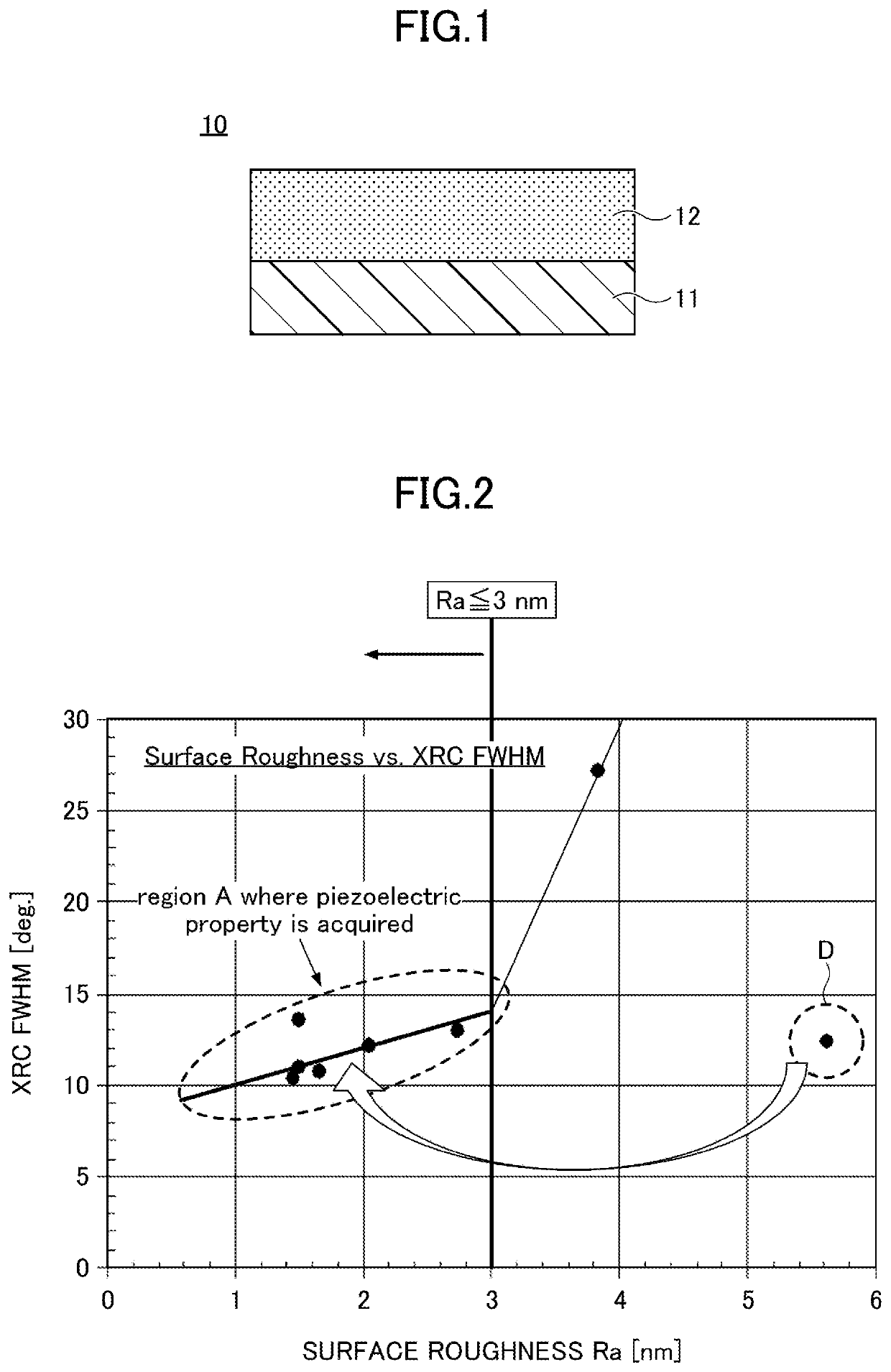
[0021]FIG. 1 is a schematic diagram of a layered structure 10 according to the first embodiment. The layered structure 10 includes a polymer substrate 11, and a crystalline functional layer 12 provided on one surface of the substrate 11. The functional layer 12 is a layer having a specific function, such as a piezoelectric layer in which micro polarization occurs in response to a pressure applied, a temperature-sensitive magnetic film whose hysteresis characteristics change depending on temperature, or a crystalline nanoporous metal oxide film having a catalytic property.

[0022]By using the polymer substrate 11, the entirety of the layered structure 10 can be made flexible. In order to increase the flexibility, it may be desirable to reduce the thickness of the functional layer 12 to such an extent not to damage the expression of the function. However, the thinner the functional layer 12, the greater the influence of the surface condition of the underlayer, and cracks penetrating thr...

second embodiment

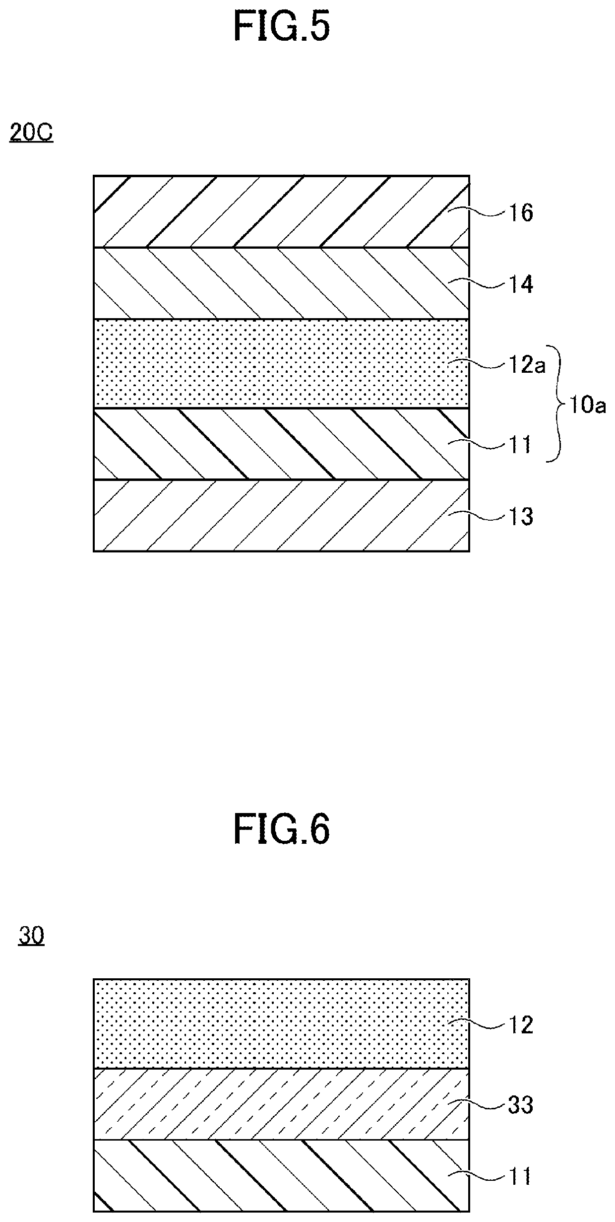
[0059]FIG. 6 is a schematic diagram of a layered structure 30 according to the second embodiment. The layered structure 30 includes a polymer substrate 11, an amorphous layer 33 provided on the substrate 11, and a crystalline functional layer 12 provided on the amorphous layer 33.

[0060]The surface roughness of the substrate 11 is 3 nm or less in arithmetic average roughness Ra. By using a polymer base material 11 having such a smooth surface, the entirety of the layered structure 30 can be made flexible and the crystal orientation of the functional layer 12 can be improved.

[0061]In the second embodiment, the crystal orientation of the functional layer 12 is further improved by inserting an amorphous layer 33 between the polymer substrate 11 and the functional layer 12. The “amorphous layer” does not have to be 100% amorphous, and it refers to a layer in which 90% or more, preferably 95% or more is amorphous, and in which the interface with the functional layer 12 is amorphous.

[0062]...

third embodiment

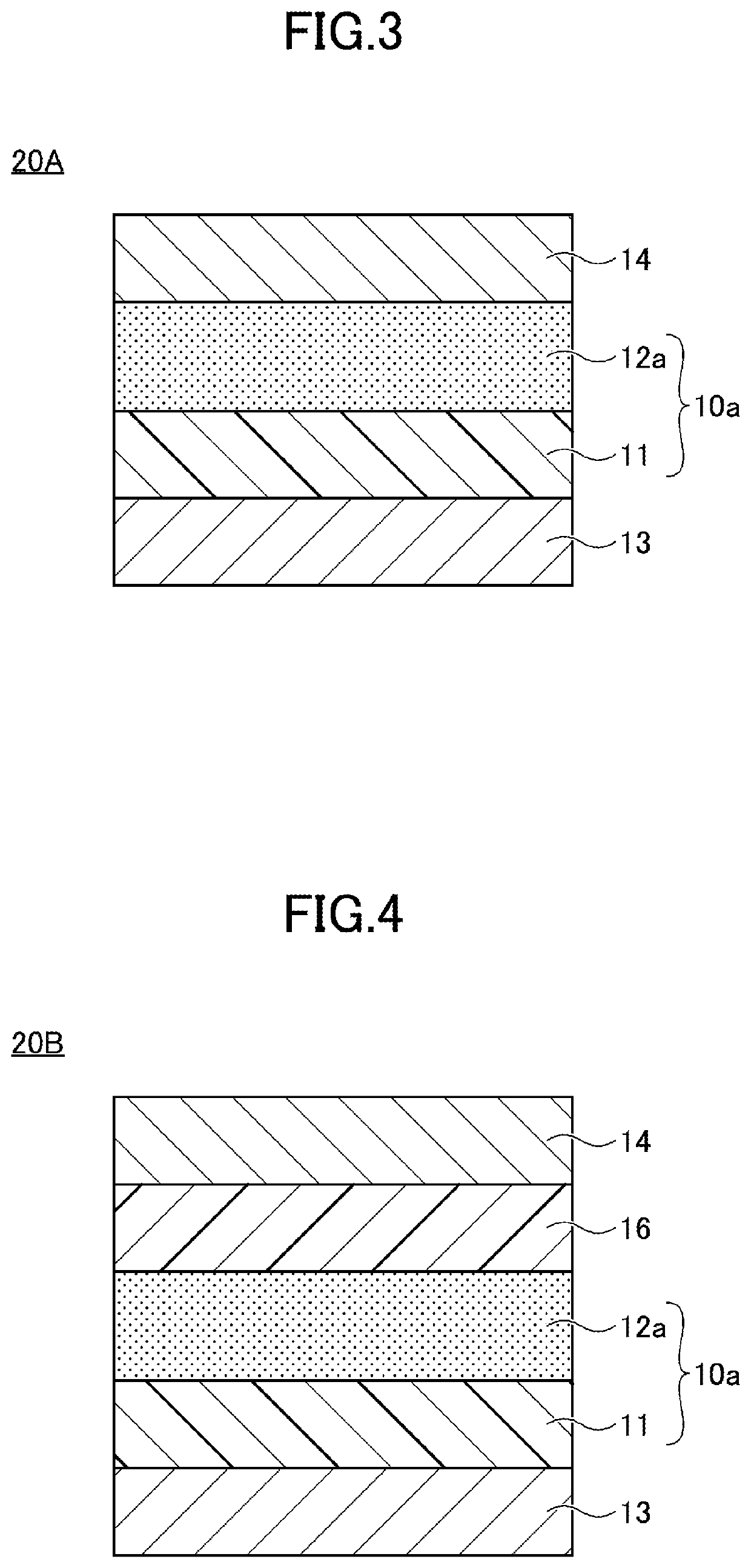
[0075]FIG. 8 is a schematic diagram of a layered structure 30b of the third embodiment and the piezoelectric device 50 using the same. The layered structure 30b includes a polymer substrate 11, an amorphous layer 33b provided on the substrate 11, a first electrode layer 13 provided on the amorphous layer 33b, and a piezoelectric layer 12a provided on the first electrode layer 13. The piezoelectric layer 12a is an example of the crystalline functional layer 12, and has a film thickness of 50 to 200 nm.

[0076]The surface roughness of the polymer substrate 11 is 3 nm or less in arithmetic average roughness Ra. By using a polymer substrate 11 with such a smooth surface, the entirety of the layered structure 30b can be flexible, and the crystal orientation of the piezoelectric layer 12a is improved.

[0077]In the third embodiment, the amorphous layer 33b is provided between the substrate 11 and the first electrode layer 13, which is provided under the piezoelectric layer 12a. The amorphous ...


PUM

PropertyMeasurementUnit
Thicknessaaaaaaaaaa
Thicknessaaaaaaaaaa
Surface roughnessaaaaaaaaaa

Abstract

The occurrence of cracking in a functional layer is suppressed, while maintaining flexibility of a layered structure. The layered structure includes a polymer substrate, and a crystalline functional layer formed on the first surface of the substrate. The surface roughness of the first surface of the substrate is 3 nm or less in terms of arithmetic mean roughness (Ra).

Description

TECHNICAL FIELD[0001]The present invention relates to a layered structure, a piezoelectric device using the same, and a method of manufacturing a piezoelectric device.BACKGROUND ART[0002]Conventionally, a piezoelectric device, which makes use of the piezoelectric effect of a substance has been adopted. The piezoelectric effect is a phenomenon in which microscopic polarization occurs in proportion to a pressure applied to a substance. Various sensors such as pressure sensors, acceleration sensors, or acoustic emission (AE) sensors for detecting elastic waves have been manufactured by utilizing the piezoelectric effect.[0003]In recent years, touch panels have been used as input interfaces of information processing devices such as smartphones, and applying piezoelectric devices to touch panels is increasing. A touch panel is integrated into the display device of an information processing device, and high transparency to visible light is required to improve the visibility. On the other ...

Claims


Application Information

Patent Timeline
IPC IPC(8): H01L41/08H01L41/047H01L41/187H01L41/29H01L41/316H01L41/319
CPCH01L41/0815H01L41/0478H01L41/319H01L41/29H01L41/316H01L41/187H10N30/877H10N30/878H10N30/853H10N30/073H10N30/076H10N30/06H10N30/079H10N30/706H10N30/708B32B7/025B32B27/06H10N30/87
Inventor NAKAMURA, DAISUKENAGAOKA, NAOKIKUROSE, MANAMIISHIKAWA, TAKETOMACHINAGA, HIRONOBU
Owner NITTO DENKO CORP
Learn More