Pattern Measurement Device and Pattern Measurement Method
a technology of pattern measurement and pattern, applied in the field of measurement technique, can solve the problems of large influence of beam angle and sample angle accuracy on the accuracy of obtained cross-sectional shape and reconstructed three-dimensional shap
- Summary
- Abstract
- Description
- Claims
- Application Information
AI Technical Summary
Benefits of technology
Problems solved by technology
Method used
Image

Examples
first embodiment
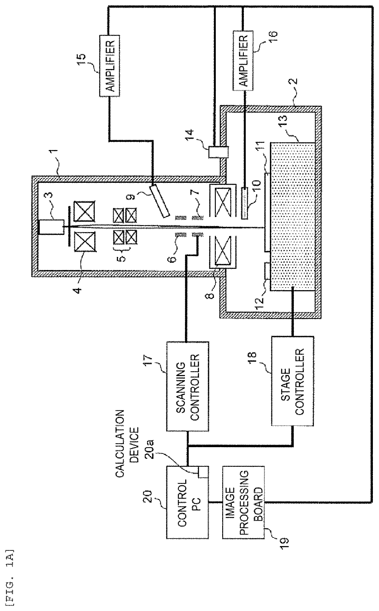
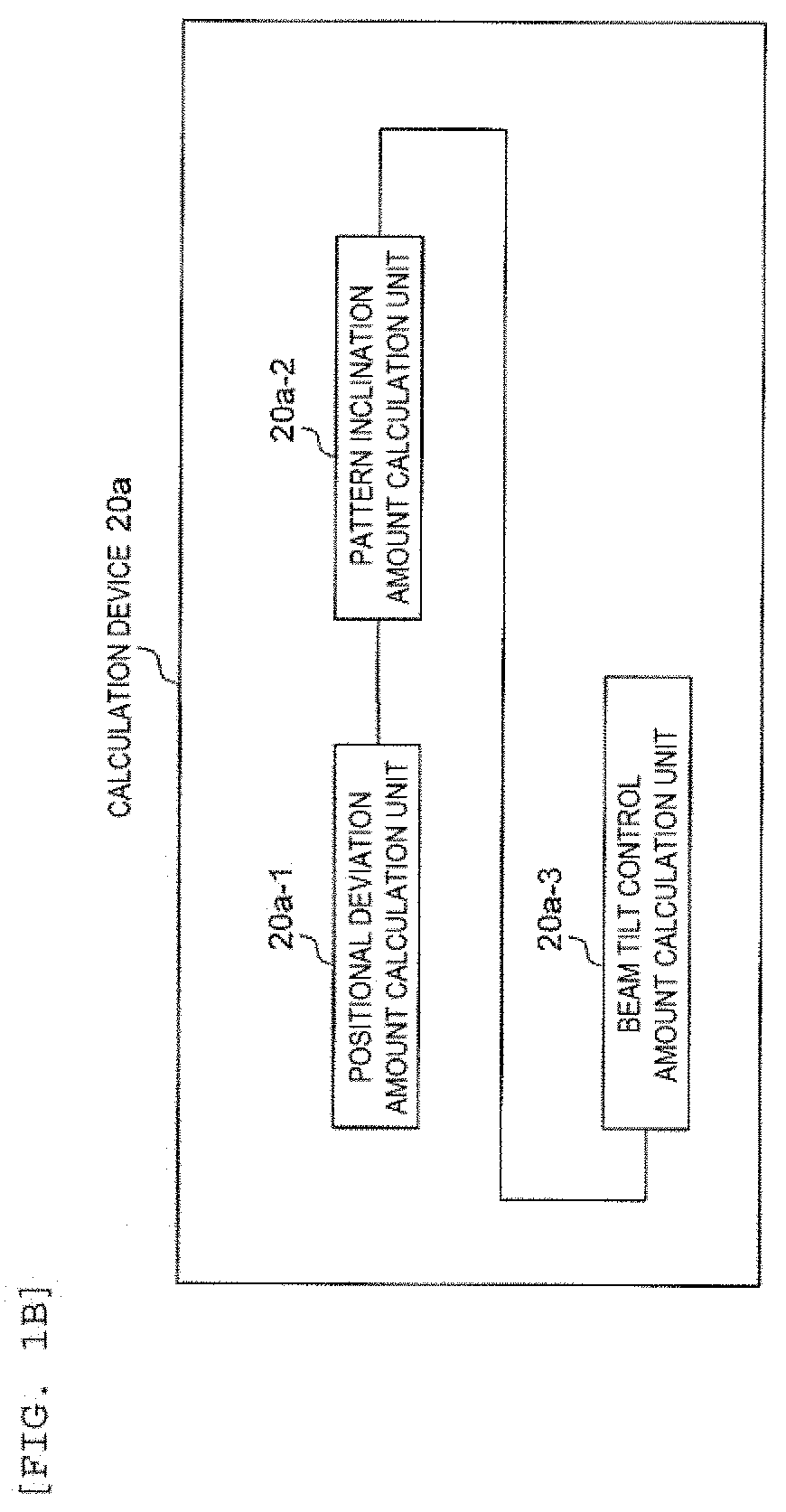
[0036]FIG. 1A is a diagram showing a configuration example of a pattern measurement device according to a first embodiment. A device main body includes a column 1, which is an electron optical system, and a sample chamber 2. The column 1 includes an electron gun 3, a condenser lens 4, an objective lens 8, a deflector 7, an aligner 5, a secondary electron detector 9, an E×B filter 6, and a back scattered electron detector 10. A primary electron beam (an irradiation electron) generated by the electron gun 3 converges and is emitted onto a wafer 11 with the condenser lens 4 and the objective lens 8. The aligner 5 aligns a position at which the primary electron beam is incident on the objective lens 8. The wafer 11 is scanned with the primary electron beam by the deflector 7. The deflector 7 scans the wafer 11 with the primary electron beam according to a signal from a beam scanning controller 17. Secondary electrons obtained from the wafer 11 by the irradiation of the primary electron ...
second embodiment
[0054]A hole pattern measurement technique using a pattern measurement device according to a second embodiment of the invention will be described below. In the case of the groove pattern shown in the first embodiment, the incident beam may be controlled only in one direction. In the case of a hole pattern shown in the second embodiment, it is necessary to control the beam inclination in both X and Y directions. In the second embodiment, a correction expression in the X direction and the Y direction is obtained, and the correction is performed in each direction.
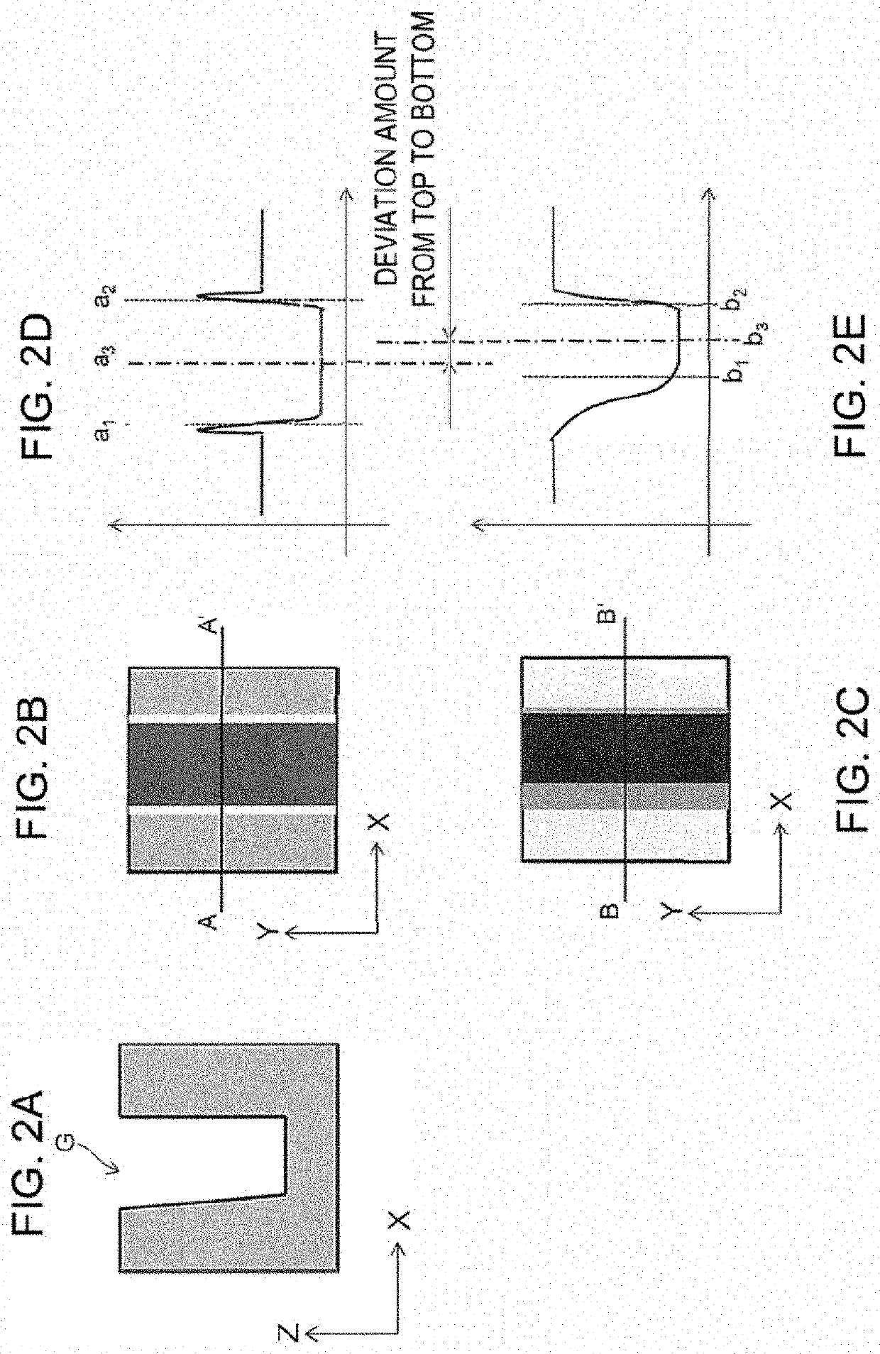
[0055]FIG. 6A(a) is a cross-sectional view of a hole-shaped pattern, and a hole H is etched with respect to the perpendicular (the Z axis) of the sample. FIG. 6A(b) illustrates, when an image is captured such that the center of the top of the hole pattern is the center of the image, a shape and a center position of the bottom of the hole pattern with respect to three beam incident angles different in the X direction. When the ...
third embodiment
[0062]In the first embodiment, the procedure of calculating the pattern inclination amount based on the measurement results of the positional deviation amount by obtaining the relational expression between the relative angle between the incident beam and the etching pattern and the positional deviation amount is described. If the shape of the etching pattern to be measured is constant, the same relational expression can be used. However, for example, when a pattern depth changes, the relational expression needs to be obtained again.
[0063]For example, as shown in FIGS. 9(a) and (b), when a depth of a layer to be etched changes from D1 to D1+ΔD, the positional deviation amount to be measured increases even if the inclination angle of the pattern is the same (−α°). That is, as shown in a graph of FIG. 9(c), a change amount (nm / deg) of the positional deviation per unit beam tilt change is different between FIG. 9(a) and FIG. 9(b). Therefore, each time the etching process is changed, re-...
PUM
| Property | Measurement | Unit |
|---|---|---|
| inclination angles | aaaaa | aaaaa |
| threshold | aaaaa | aaaaa |
| threshold | aaaaa | aaaaa |
Abstract
Description
Claims
Application Information
 - R&D
- Intellectual Property
- Life Sciences
- Materials
- Tech Scout
- Unparalleled Data Quality
- Higher Quality Content
- 60% Fewer Hallucinations
Browse by: Latest US Patents, China's latest patents, Technical Efficacy Thesaurus, Application Domain, Technology Topic, Popular Technical Reports.
© 2025 PatSnap. All rights reserved.Legal|Privacy policy|Modern Slavery Act Transparency Statement|Sitemap|About US| Contact US: help@patsnap.com