Deep reactive ion etching process for fluid ejection heads

a technology of reactive ions and fluid ejection heads, which is applied in the direction of separation processes, instruments, filtration separation, etc., can solve the problems of difficult to provide a reproducible shelf width wb>2/b>, inability to maintain a stable thermal environment, and time-consuming and problematic, so as to improve the protection of the fluid ejector stack, simplify the wafer inspection, and reduce the rough edge of the fluid supply vias

Active Publication Date: 2022-09-08
FUNAI ELECTRIC CO LTD
View PDF0 Cites 0 Cited by
  • Summary
  • Abstract
  • Description
  • Claims
  • Application Information

AI Technical Summary

Benefits of technology

[0005]Maintaining a suitable shelf width W2 is time-consuming and problematic in the production of ejection head chips. The shelf width W2 requirement has constrained the design of wider fluid supply slots 14 using DRIE etch techniques. Conventional wisdom has required the silicon shelf width W2 be sufficient to prevent the metal layers, such as the tantalum layer 30 from being exposed to fluids ejected by the ejection head. Historically, the shelf width W2 has varied between about 3 and about 20 microns. It has been difficult to provide a reproducible shelf width W2 due to a number of factors including, but not limited to, mask resolution and bias, alignment issues with the mask and the substrate, inability to maintain a stable thermal environment in the DRIE chamber which produces undercutting and over-etching of the silicon substrate, and post etch residue cleanup. Accordingly, the requirement for a silicon shelf 40 has resulted in time consuming expensive and highly detailed automated measurement processes that have increased production time and production costs. Over-etched shelves 40 have been known to propagate the length of the fluid supply via 14 resulting in reduced ejection head chip 10 strength when used with various solvent-based fluids. Thus, the difficulties in maintaining the integrity of the silicon shelf 40 have resulted in a reduced yield of usable ejection head chips 10 from a silicon wafer 12. What is needed therefore, is an ejection head chip design that reduces or eliminates the reliance on the silicon shelf 40 to protect the metal layers from corrosion due to contact with fluid ejected by the ejection head. There is also a need for wider fluid supply vias 14 for increased fluid flow to the fluid ejectors 18 without increasing the overall size of the ejection head chip 10.
[0012]An advantage of using the encapsulating material for protecting the metal layer in the fluid ejector stack is that the need for a silicon shelf between the fluid supply via and the fluid ejector stack is reduced thereby greatly simplifying wafer inspection. Edge roughness of the fluid supply vias may also be reduced due to improved protection of the fluid ejector stack. The fluid via width may be increased to provide increased fluid refill rates for the fluid chambers by reducing the width of the silicon shelves in the x direction adjacent to the fluid supply vias.

Problems solved by technology

Maintaining a suitable shelf width W2 is time-consuming and problematic in the production of ejection head chips.
It has been difficult to provide a reproducible shelf width W2 due to a number of factors including, but not limited to, mask resolution and bias, alignment issues with the mask and the substrate, inability to maintain a stable thermal environment in the DRIE chamber which produces undercutting and over-etching of the silicon substrate, and post etch residue cleanup.
Accordingly, the requirement for a silicon shelf 40 has resulted in time consuming expensive and highly detailed automated measurement processes that have increased production time and production costs.
Thus, the difficulties in maintaining the integrity of the silicon shelf 40 have resulted in a reduced yield of usable ejection head chips 10 from a silicon wafer 12.

Method used


Image

  • Deep reactive ion etching process for fluid ejection heads
  • Deep reactive ion etching process for fluid ejection heads
  • Deep reactive ion etching process for fluid ejection heads

Examples


Embodiment Construction

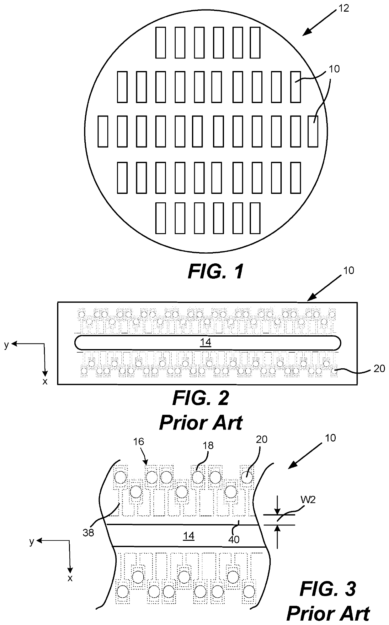
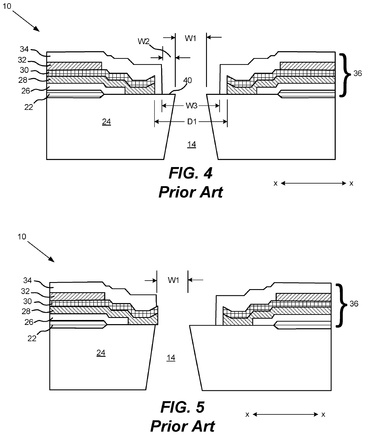
[0018]As shown in FIGS. 4-5, the maximum entrance width or the fluid supply via 14 for the prior art fluid ejector stack 36 ranges from about 60 (W1) to about 520 microns (W3). Such fluid supply width is maintained in order to prevent under-etching the fluid ejector stack 36 as shown in FIG. 5 and expose the metal layer 30 to corrosion from the fluid ejected by the ejection head.

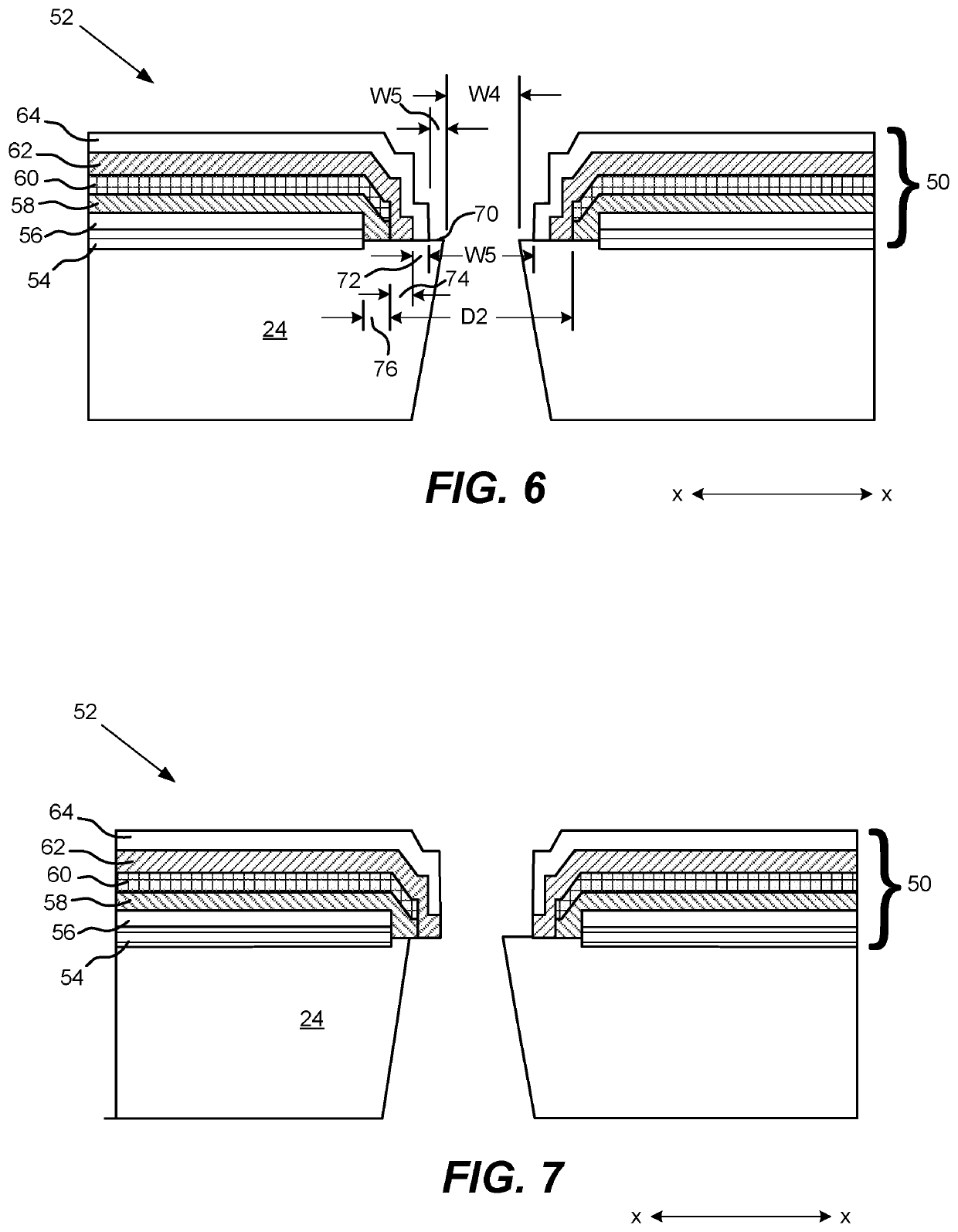
[0019]In order to better protect the metal layer 30 so that the reliance on the silicon shelf is reduced, an improved fluid ejector stack 50 for an ejection head chip 52 is provided in FIGS. 6-7. The fluid ejector stack 50 is shown in cross-sectional view in they direction through the fluid supply via 14.

[0020]Like the prior art ejection head chip 10, the ejection head chip 52 includes a first layer field oxide layer 54 adjacent to the silicon substrate 24. Next, an insulating layer 56 that may be a doped glass layer such as a phosphorus-doped silicon glass layer is deposited or grown on the field oxide laye...


PUM

PropertyMeasurementUnit
widthaaaaaaaaaa
widthaaaaaaaaaa
thicknessaaaaaaaaaa

Abstract

An ejection head chip and method for a fluid ejection device and a method for reducing a silicon shelf width between a fluid supply via and a fluid ejector stack. The ejection head chip includes a silicon substrate and a fluid ejector stack deposited on the silicon substrate, wherein at least one metal layer of the fluid ejector stack is isolated from a fluid supply via etched in the ejection head chip by an encapsulating material.

Description

TECHNICAL FIELD[0001]The disclosure is directed to micro-electro-mechanical (MEMS) devices and in particular to an improved fluid jet ejection head and method for fabricating the fluid jet ejection head.BACKGROUND AND SUMMARY[0002]Fluid jet ejection heads are used in a wide variety of application including, but not limited to, ink jet ejection heads, digital fluid dispensing devices, and pharmaceutical jet spray devices. A primary component of the fluid jet ejection device is a MEMS device that is made silicon substrate having metal and non-metal layers deposited thereon. A plurality of ejection head chips 10 are formed on silicon wafer 12 using a variety of deposition and etching processes. Once, fully formed, a nozzle plate is attached to the ejection head chips 10, and the ejection head chips are excised from the silicon wafer 12 and attached to a fluid cartridge.[0003]Each fluid jet ejection head chip 10 includes a fluid supply via 14 therein for feeding fluid to a fluid chamber...

Claims


Application Information

Patent Timeline
Patent Type & Authority Applications(United States)
IPC IPC(8): B81C1/00B81B1/00B41J2/14B41J2/16
CPCB81C1/00087B81B1/002B41J2/14B41J2/1629B41J2/162B81B2201/052B81B2203/0353B81C2201/0132B41J2/1433B41J2/14129B41J2/1603B41J2/1628B41J2/1642B41J2/1631
Inventor BERNARD, DAVID L.
Owner FUNAI ELECTRIC CO LTD
Why Eureka
Try Eureka