
A method of forming a device structure

Pending Publication Date: 2022-09-15
NEWSOUTH INNOVATIONS PTY LTD
View PDF0 Cites 0 Cited by
  • Summary
  • Abstract
  • Description
  • Claims
  • Application Information

AI Technical Summary

Benefits of technology

The present invention provides a structured connector for positioning on a device component and an elongated recess for receiving a portion of a structured wire. The connector has projections and recesses that help secure it within a polymeric material of a contact sheet or an embedding process. The invention also provides a method for embedding a portion of a structured wire into a polymeric material such that the wire is embedded securely and securely positioned.

Problems solved by technology

The grid electrode can also be formed by plating metal such as nickel, copper (Cu) and / or silver (Ag), which can result in reduced metal material costs and very narrow metal fingers, however is less commonly used due to being a less established process.
The soldering process requires localized heating and pressure, which can result in microcracks in the silicon wafers and is of particular concern when thin silicon wafers (e.g., <160 μm) are used in order to reduce the silicon material cost.
Another undesirable aspect of this interconnection process is that typically the conductive tabbing wire used to interconnect adjacent cells in a module is coated in a lead (Pb)-based alloy to ensure a low melting point and reduce the temperature at which the soldering can be performed.
It is undesirable to use lead in manufactured products due to its deleterious effect on humans and other species.
Lead-free solders can alternatively be used; however, these alloys typically require soldering at higher temperatures which is also undesirable.
Although soldering busbar interconnections have been an industrially-accepted way of interconnecting solar cells for many years, the increased photo-generated current achieved in more recently manufactured cells due to their larger areas and improved energy conversion efficiencies has made it more challenging to reduce power losses due to series resistance.
However, these performance and cost advantages are offset by increased complexity of the automated tabbing processes due to the stricter requirements for alignment of thinner busbars.
Furthermore, adhesion of the busbars can be impacted by the reduced cell contact area for each individual busbar.
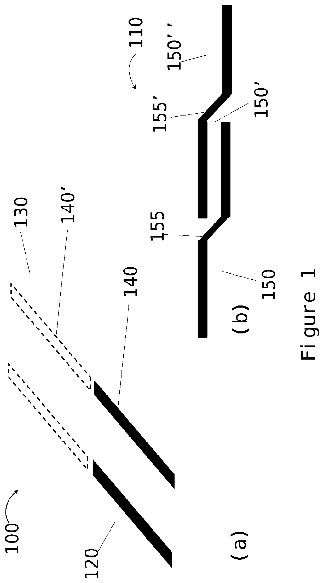
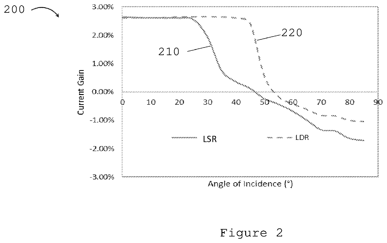
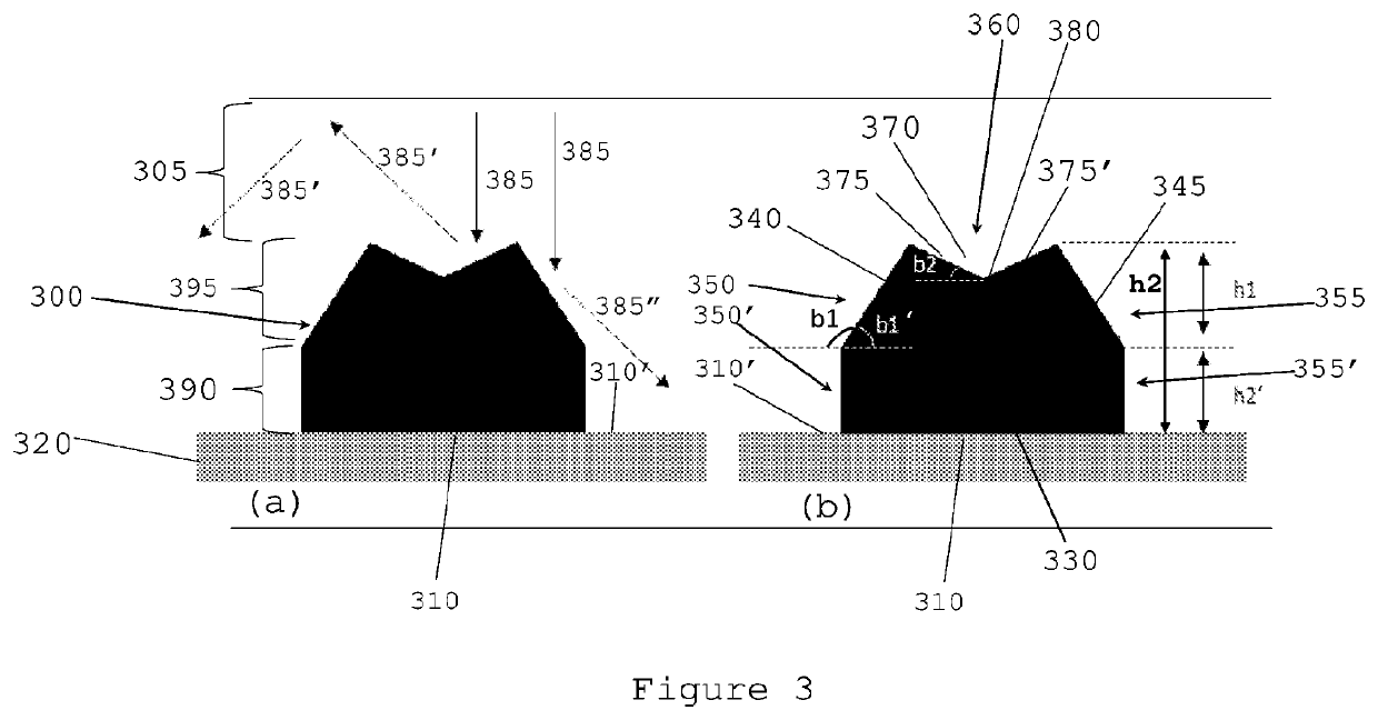
Furthermore, the use of circular wires in place of flat tabs of interconnection wire can result in increased trapping of light in the underlying cells of a module as rays impinging on the curved surface are reflected back to the front glass at a more oblique angle resulting in a higher probability of the rays being totally internally reflected back into the cell thereby increasing the probability of being absorbed in the solar cell resulting in increased photocurrent.
However, these alternative processes can also present some disadvantages.
Typically, they result in an increased interconnection cost to silicon solar module producers compared to the more traditionally-used soldering of tabbing wire.
These costs can arise due to the use of indium-containing metal alloys and the adhesive polymer sheets (in the case of SWCT), and expensive proprietary tabbing equipment or mechanical actuators required to perform the interconnection processes at the manufacturers' factories.
Part of the complexity required by the wire processing equipment arises due to the use of continuous preformed wires.
The use of wires also limits the flexibility of the interconnection arrangement.
The high costs of wire-based interconnection schemes that rely on metal alloy bonding during lamination arise in part because the entire surface of the alloy-coated wires must be coated with the metal alloy material.
This factor results in increased material costs, which can be considerable if expensive metals (e.g., indium) must be used to achieve reliable bonding to the metal fingers on the solar cell.

Method used


Image

  • A method of forming a device structure
  • A method of forming a device structure
  • A method of forming a device structure

Examples


Embodiment Construction

[0094]Embodiments of the present invention thus relate generally to structured connectors, i.e. connectors having a non-circular cross-sectional shape, for positioning on, and electrically coupling to, a surface a device component, such as a solar cell, whereby the structured connectors further allow connecting device components, such as solar cells, within a device structure, such as a photovoltaic module.

[0095]Further, embodiments of a method for forming a device structure will be described, the method allowing the interconnection of device components within the device structure by means of structured connectors as provided in accordance with embodiments of the present invention.

[0096]In the following description, embodiments of a structured connector will in particular be described in relation to a solar cell structured connector for interconnecting solar cells within a photovoltaic module. Embodiments of a structured connector in relation to a method of forming a photovoltaic mo...


PUM


Abstract

The present disclosure provides a method of forming a device structure. The method comprises providing at least one device component having front and rear device component surfaces and having at least one electrically conductive region on at least one of the device component surfaces. The method further comprises providing at least one contact sheet comprising a polymeric material and at least one electrically conductive element that has a non-circular cross-sectional shape and is embedded in the polymeric material in a manner such that a surface portion of the at least one electrically conductive element is exposed. The method also comprises applying a bonding material to either one or both of the exposed surface portion and at least one of the electrically conductive regions on the at least one of the device component surfaces. In addition, the method comprises positioning the at least one contact sheet relative to the at least one device component such that the bonding material is located between the at least one electrically conductive region and the exposed surface portion. Further, the method comprises activating the bonding material such that a bond and an electrically conductive coupling is formed between the at least one electrically conductive region and the exposed surface portion.

Description

TECHNICAL FIELD OF THE INVENTION[0001]The present invention relates to a method of forming a device structure.BACKGROUND OF THE INVENTION[0002]Most solar modules that are used to convert sunlight into electricity comprise arrays of silicon-based solar cells. The individual solar cells are typically fabricated using doped crystalline silicon wafers and include electron-collecting and hole collecting regions. These carrier-collecting regions can be formed by solid state diffusion or by the application of surface layers that can selectively collect one carrier polarity when the solar cell is illuminated. In order to extract the photo-generated electrical carriers from the solar cell, conductive regions comprising metal electrodes (or contacts) are typically formed in contact with the electron and hole-contacting regions of the cell. Conducting wires can then be bonded or connected to these metal electrodes enabling the individual solar cells to be connected into arrays of solar cells c...

Claims


Application Information

Patent Timeline
IPC IPC(8): H01L31/05H01L31/02H01L31/048
CPCH01L31/0512H01L31/02008H01L31/048H01L31/0508H01L31/022433H01L31/0481H01L31/0547
Inventor SONG, NINGLI, YANGLENNON, ALISON JOANHSIAO, PEI-CHIEHOUYANG, ZIHALL, CHARLES ARAM MANDELA
Owner NEWSOUTH INNOVATIONS PTY LTD
Features
  • Generate Ideas
  • Intellectual Property
  • Life Sciences
  • Materials
  • Tech Scout
  • Unparalleled Data Quality
  • Higher Quality Content
  • 60% Fewer Hallucinations
Learn More