A translucent photovoltaic device and a method for manufacturing thereof

a photovoltaic device and translucent technology, applied in the direction of photovoltaic energy generation, semiconductor devices, electrical equipment, etc., can solve the problems of reducing the efficiency of the whole pv device, and substantially high-efficiency pv devices

Pending Publication Date: 2022-09-15
SAULE SPOLKA AKCYJNA
View PDF5 Cites 0 Cited by
  • Summary
  • Abstract
  • Description
  • Claims
  • Application Information

AI Technical Summary

Benefits of technology

This patent is about a new type of photovoltaic device that is see-through. The patent also describes a method for making this new device. This invention is useful because it allows for the creation of a see-through photovoltaic device that is both efficient and visually appealing.

Problems solved by technology

Although the laser ablation provides the required translucency of the PV devices, it removes a part of the working material of the PV cell thereby providing decreased efficiency of the whole PV device.
Nonetheless, this drawback becomes negligible when it comes to substantially high-efficient PV devices, such as those having perovskite photoactive layers.
Nevertheless, the drawback which does remain important in the field of translucent PV devices is associated with the method of the ablation itself, and hence the characteristic of formed see-though apertures providing translucency.
Also, depending on the material used, some of the translucent PV devices show red-color high transparency, which limits their range of applications.
Nonetheless, the patterning P4 does not remove the front contact layer, i.e. the electrode disposed directly on the semi-transparent substrate.
Therefore, the light-transmissive apertures of that device are not fully surrounded by the layer stack layers that contribute to the power conversion (in particular, in view of delamination of the top metal electrode during the laser ablation, the P4 surrounding is non-active).
This publication further describes the drawbacks of both methods, providing that laser patterning causes damages, i.e. delamination of functional layers of the PV device.
Nonetheless, the presented method involves a complex multi-step laser method for forming separately first and second light-transmissive apertures.
Furthermore, the light-transmissive apertures of that device are not fully surrounded by the layer stack layers that contribute to the power conversion (in particular, in view of lack of top electrode in the surrounding of the aperture, its surrounding is non-active).
However, the PV module according to U.S. Pat. No. 4,795,500 has drawbacks, namely problems of short circuit and leakage current due to the high temperature laser cutting process.

Method used


Image

  • A translucent photovoltaic device and a method for manufacturing thereof
  • A translucent photovoltaic device and a method for manufacturing thereof
  • A translucent photovoltaic device and a method for manufacturing thereof

Examples


Embodiment Construction

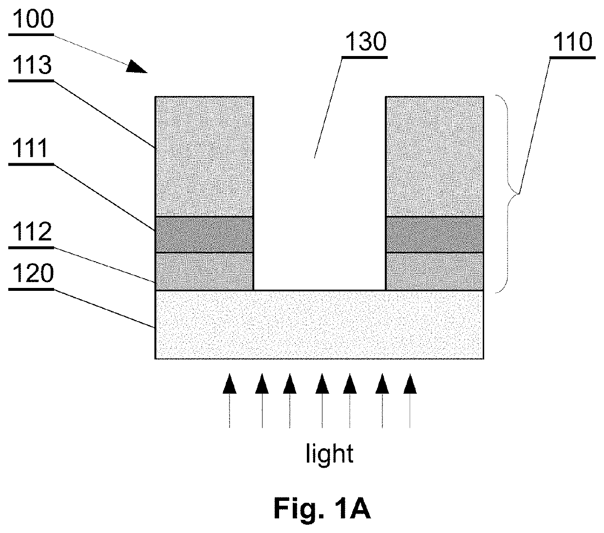
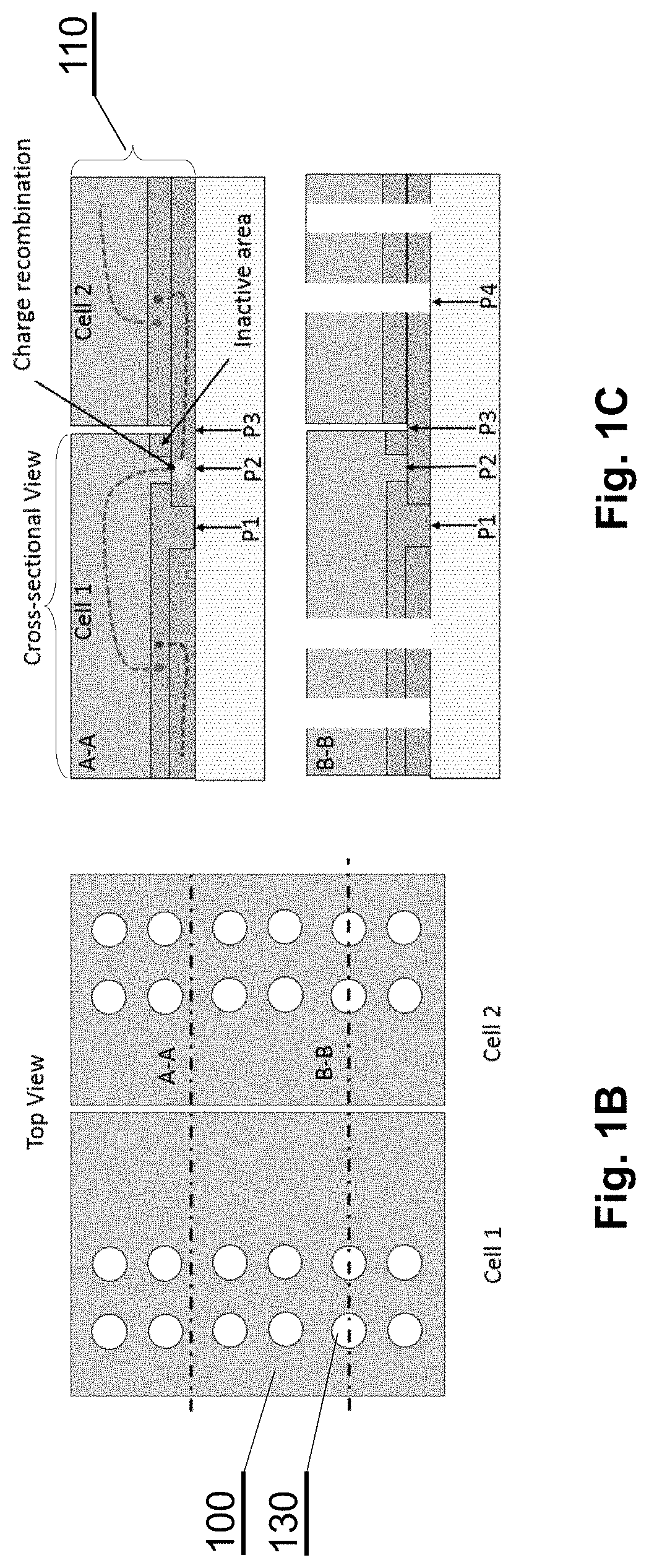
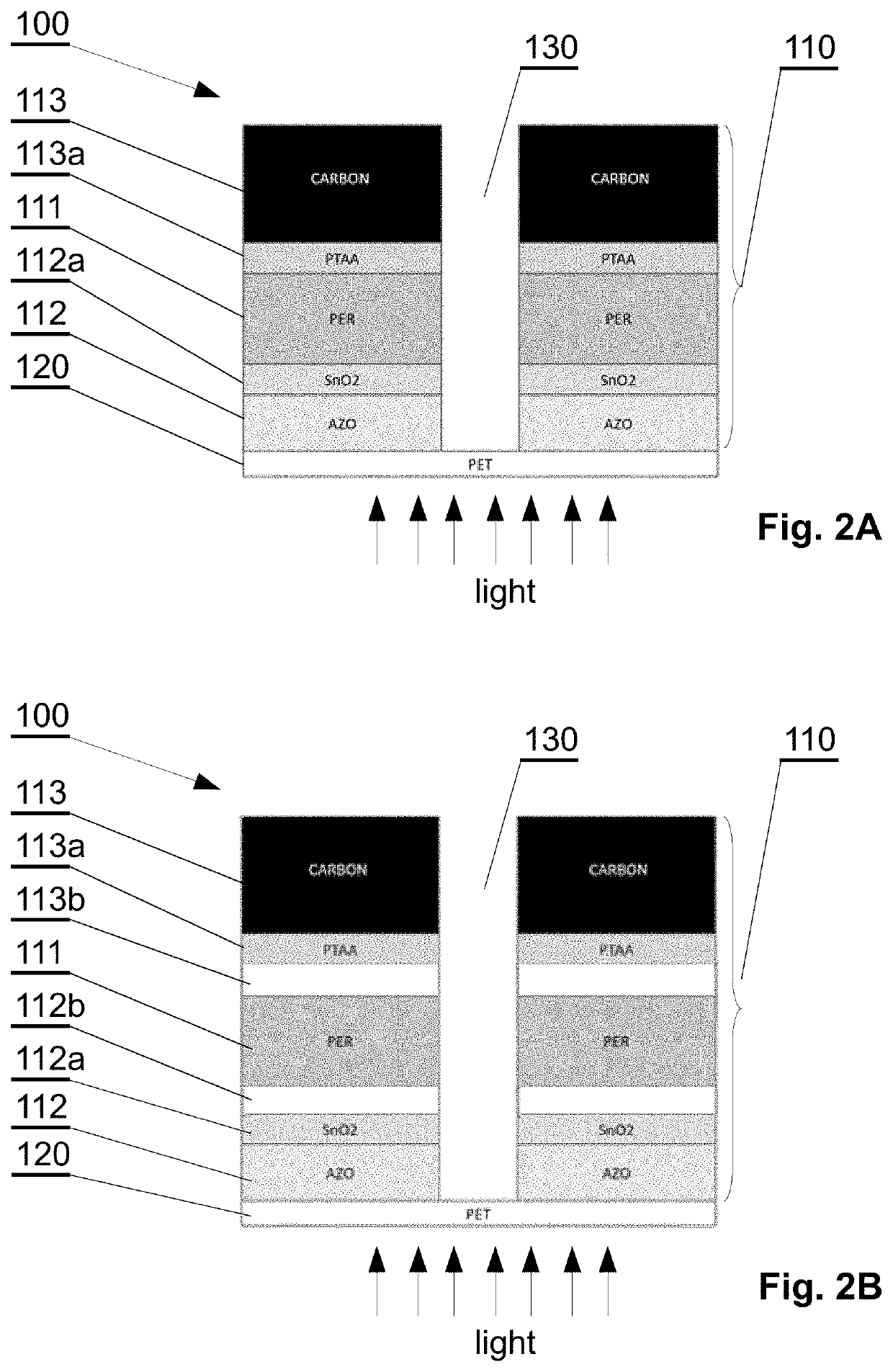
[0032]The developed method for manufacturing a translucent photovoltaic (PV) device allows one to obtain the PV devices comprising light-transmissive apertures of improved quality. Especially, the obtained apertures do not comprise metallic impurities and feature a regular shape, without significant delamination effect. Due to the above features, the short-circuits are not observed for the obtained PV devices. Moreover, the developed method is simplified and it may be accomplished with the use of less expensive nanosecond lasers for forming the light-transmissive apertures, instead of expensive picosecond or femtosecond lasers used for performing such the apertures according to the known solutions.

[0033]Although a nanosecond laser is characterized by a much larger heat affected zone than a picosecond laser, due to the structure of the PV device according to the present invention (having a carbon back electrode), the carbon electrode will combust and will not contact (bridge) with th...


PUM

PropertyMeasurementUnit
thicknessaaaaaaaaaa
areaaaaaaaaaaa
thicknessaaaaaaaaaa

Abstract

A translucent photovoltaic (PV) device comprising a semi-transparent substrate 120 and at least one translucent photovoltaic (PV) cell 100, the PV cell 100 comprising a stack 110 of layers disposed on the substrate 120, the stack 110 comprising: a front electrode layer 112, a back electrode layer 113, and a perovskite photoactive layer 111 between the anode layer and the cathode layer. The back electrode layer 113 comprises carbon, wherein the stack 110 of layers comprises laser-made light-transmissive apertures 130 extending through at least the back electrode layer 113 and the perovskite photoactive layer 111 wherein the light-transmissive apertures 130 are fully surrounded by the layer stack 110 layers that contribute to the power conversion.

Description

TECHNICAL FIELD[0001]The present disclosure relates to a translucent photovoltaic device and a method for manufacturing thereof.BACKGROUND[0002]Thin film perovskite photovoltaic (PV) devices are attractive due to their high absorption coefficient, high power conversion efficiencies, low weight and high-speed production capabilities.[0003]Desirable features of these devices are semi-transparency or translucency, which are related to the constant increase in energy consumption. Semi-transparent and translucent PV devices, especially those of low weight and preferably flexible, are suitable to be applied on the windows and other see-through surfaces. Hence, these kinds of PV devices may cover not only the opaque surfaces (as roofs or walls), but they can take a form of glass walls of buildings, stickers for the cars windows and car bodies, as well as forms of casings for cell-phones, tablets, laptops, as well as other electronic devices.[0004]The semi-transparency / translucency of the p...

Claims


Application Information

Patent Timeline
Patent Type & Authority Applications(United States)
IPC IPC(8): H01L51/42H01L27/30H01L51/00H10K99/00
CPCH01L51/4253H01L27/302H01L51/0009H01L51/4226H10K30/57H10K71/162H10K30/50H10K85/50H10K39/12Y02E10/549H10K71/60H10K30/30H10K30/151
Inventor BABU, VIVEKFORGACS, DAVID
Owner SAULE SPOLKA AKCYJNA
Why Eureka
Try Eureka