
Four device SRAM cell with single bitline

a technology of sram cell and bitline, which is applied in the direction of static storage, information storage, digital storage, etc., can solve the problems of insufficient pull-up and/or high level within the cell, and the recovery time of these resistors is far too slow

Inactive Publication Date: 2000-01-04
IBM CORP
View PDF1 Cites 26 Cited by
  • Summary
  • Abstract
  • Description
  • Claims
  • Application Information

AI Technical Summary

Benefits of technology

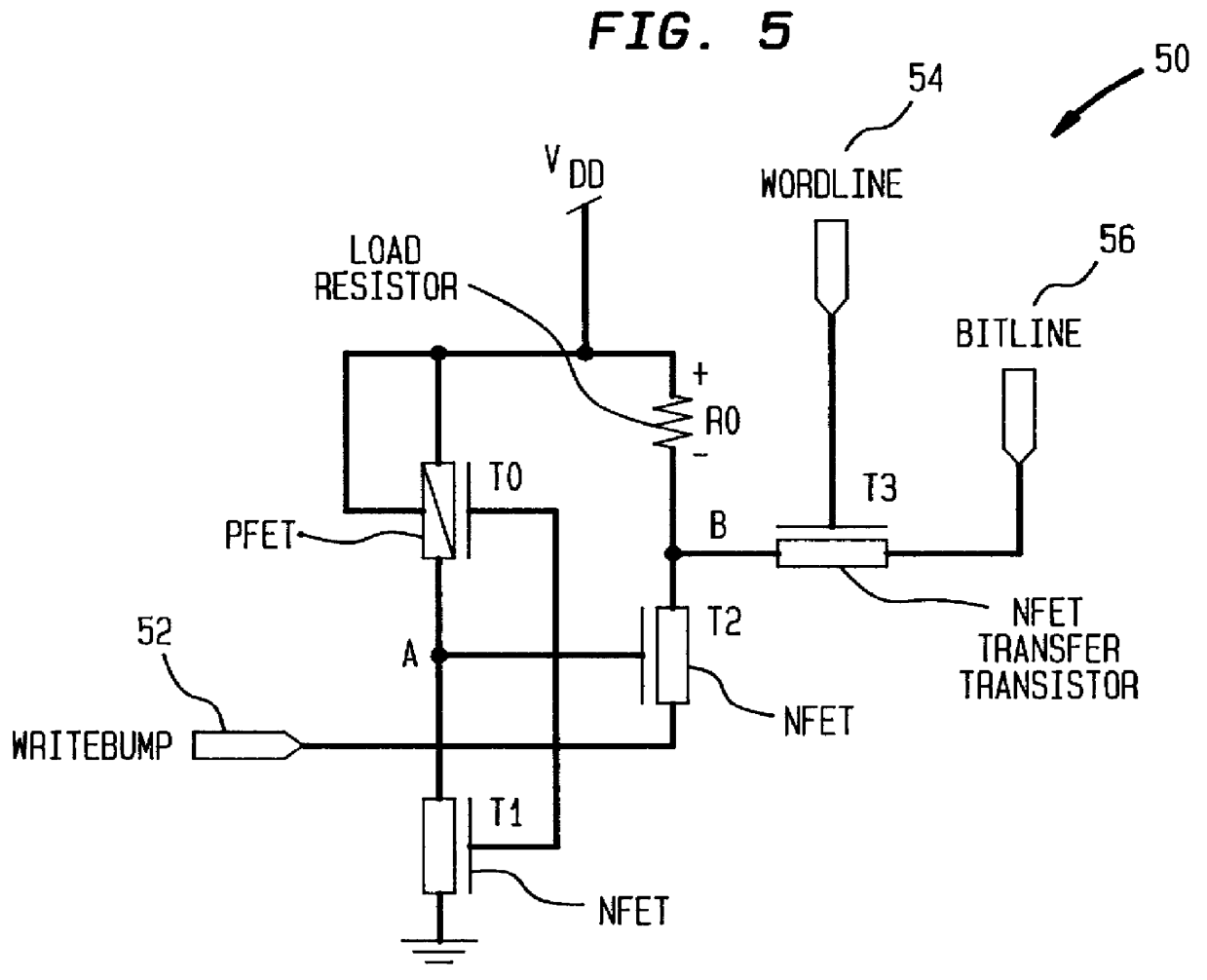
A main advantage of the present invention is its small size. One less bitline and transfer transistor offers substantial array area savings at a time in the semiconductor industry / art when entire processors and memory are competing for the same silicon. The present invention advantageously overcomes the problems faced by the single ended five device predecessor. The `WRITEBUMP` port 52 simplifies writing a `1` and makes the `WRITE` operation more reliable than had previously been accomplished. Further reduction in cell size with the substitution of one of the two PMOS load transistors in the single ended five transistor CMOS SRAM cell (FIG. 2) with a poly load / pullup resistor (FIG. 5--four transistor CMOS SRAM cell) offers an additional level of silicon density improvement without any significant adverse performance impact and with less power dissipation than the more common two resistor R-load cell (FIG. 3).

Problems solved by technology

Therefore, the recovery time of these resistors is far too slow to adequately pull-up and / or maintain stable high levels within the cell 40.

Method used


Image

  • Four device SRAM cell with single bitline
  • Four device SRAM cell with single bitline
  • Four device SRAM cell with single bitline

Examples


Embodiment Construction

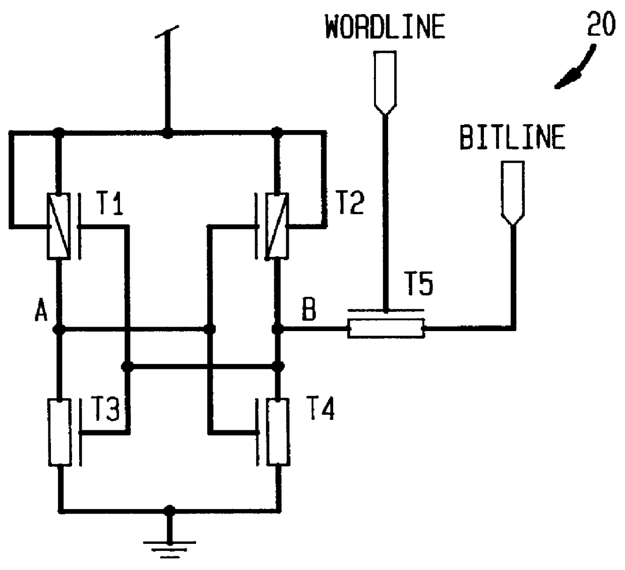
Turning now to FIG. 5, a single ended four transistor SRAM CMOS cell 50 in accordance with the present invention contains one less transistor than the more conventional five transistor device single ended CMOS SRAM cell 20 as shown and discussed herein above with reference to FIG. 2. In the single ended four transistor SRAM CMOS cell 50 in accordance with the present invention, one of two PFET load devices has been replaced with a polysilicon load resistor R0 to reduce the cell size further. Furthermore, a reliable write access into the cell 50 is provided by the addition of a `WRITEBUMP` port 52 into each cell 50 within an SRAM cell memory array.

A `WRITEBUMP` signal includes a one-shot pulse, generated off a rising edge of the logical AND of a `WRITE ENABLE` signal and a decoded `WORDLINE` signal. That is, for every row of cells sharing a common wordline 54, there is a corresponding `WRITEBUMP` pulse generated from its respective wordline and write enable. When a row of cells along...


PUM


Abstract

A memory cell includes a static inverter having an input connected to a storage node. An impedance connects the storage node to a voltage supply. A first transistor, having an input connected to an output of the static inverter, connects the storage node to a write line. Lastly, a second transistor, responsive to a wordline access signal, connects the storage node to a single data bitline. The memory cell further includes a single ended four transistor CMOS SRAM cell. Additionally, a memory array is disclosed which includes a plurality of memory cells arranged to form a matrix of rows and columns, each memory cell including a single ended four transistor CMOS SRAM cell.

Description

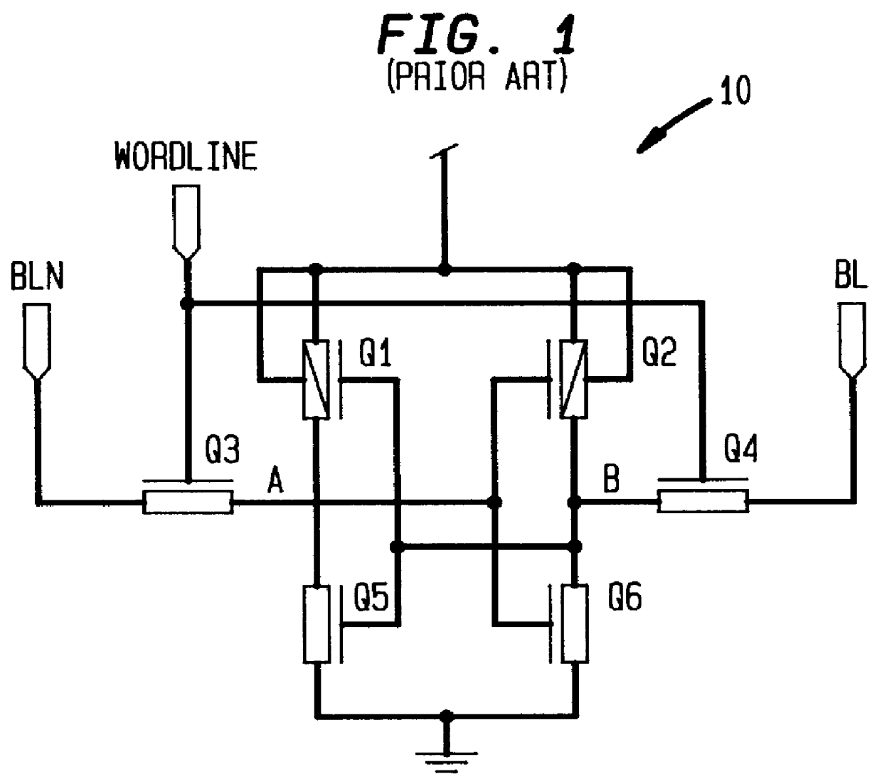
1. Field of the InventionThis invention relates generally to static memory devices and, more particularly, to a four device static random access memory device having a single bitline.2. Discussion of the Related ArtVarious configurations of static random access memory (SRAM) memory cells have been designed / developed to reduce silicon area by eliminating devices where smaller array size is needed. FIG. 1 illustrates a basic six transistor full CMOS SRAM cell 10, as is known in the art. Data is stored in the cell 10 as voltage levels with the two sides of a bistable transistor flip-flop (i.e., latch) in opposite voltage configurations. For example, node A is high and node B is low in one state; whereas, node A is low and node B is high in the opposite state resulting in two stable states (i.e., bistable).One approach taken to reduce the basic six transistor full CMOS cell is shown in FIG. 2. FIG. 2 shows a single-ended five transistor static CMOS cell 20. The five transistor CMOS cell...

Claims


Application Information

Patent Timeline
IPC IPC(8): G11C11/41
CPCG11C11/41G11C11/413
Inventor BATSON, KEVIN ARTHURROSS, JR., ROBERT ANTHONY
Owner IBM CORP
Learn More