Method of batch testing surface mount devices using a substrate edge connector

a technology of edge connector and surface mount device, which is applied in the direction of individual semiconductor device testing, semiconductor/solid-state device testing/measurement, instruments, etc., can solve the problem of design achieve the effect of reducing the handling of individual devices, reducing cost and handling damag

Inactive Publication Date: 2000-02-01
SEMICOA CORP
View PDF16 Cites 25 Cited by
  • Summary
  • Abstract
  • Description
  • Claims
  • Application Information

AI Technical Summary

Benefits of technology

The design reduces handling of the individual devices. The invention allows all of the testing and assembly to be done in a "batch" fashion. The board that is used to test the devices is separated to create the package for the individual components. The technique of the invention reduces cost and handling damage.

Problems solved by technology

The design reduces handling of the individual devices.

Method used


Image

  • Method of batch testing surface mount devices using a substrate edge connector
  • Method of batch testing surface mount devices using a substrate edge connector
  • Method of batch testing surface mount devices using a substrate edge connector

Examples


Embodiment Construction

The present invention is a method and apparatus for batch testing of surface mount semiconductor devices. In the following description, numerous specific details, such as number of devices, substrate type, etc., are set forth in detail in order to provide a more thorough description of the present invention. It will be apparent, however, to one skilled in the art, that the present invention may be practiced without these specific details. In other instances, well-known features have not been described in detail so as not to obscure the present invention.

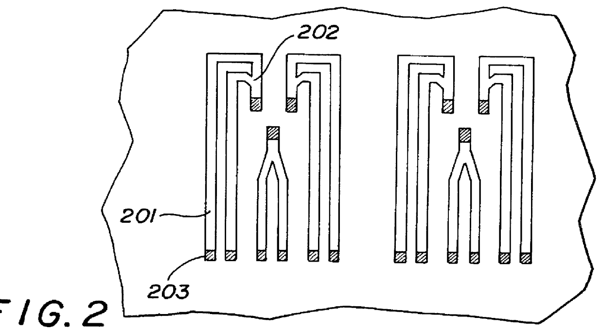
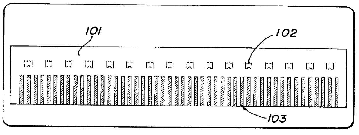
The continuing trend of reducing the size of electronic devices has resulted in the development of increasing smaller semiconductor device packages, including small outline transistor (SOT) packages. These small packages are difficult and expensive to test and burn-in individually. The present invention provides a solution to these problems. The present invention uses a ceramic substrate board that contains a plurality of packaged de...


PUM


Abstract

The present invention is used with single devices mounted on a ceramic substrate. The devices are broken out of the sheet, after all testing, electrical conditioning, and screening, as small surface mount devices. Conductive strips are formed on the ceramic substrate and are spaced to match a standard circuit board edge connector. These strips are electrically connected to the devices to allow testing and burn-in in sheet form rather than testing each device individually. The design reduces handling of the individual devices. The invention allows all of the testing and assembly to be done in a "batch" fashion. The board that is used to test the devices is separated to create the package for the individual components. The technique of the invention reduces cost and handling damage.

Description

1. Field of the InventionThis invention is directed to batch testing of semiconductor devices.2. Background ArtAs part of the manufacture of semiconductor devices, it is desired to test the devices so that inoperative devices can be identified and disposed of. Testing can occur at many times during the process of manufacture. For example, semiconductor devices are sometimes manufactured in bulk as a plurality of die on a substrate (referred to as a "wafer"). A "grid" of devices on the wafer are created, and each die is coupled to a test circuit using probes. Inoperative or substandard die are identified by results of the testing process and are marked as "bad" or "rejected". After this initial testing, the die are individually broken off the wafer and are "packaged" in a form for distribution. At this time, the packaged devices are individually tested again so that only operative devices are delivered. This individual testing of packaged devices is time consuming. It is desired to p...

Claims


Application Information

Patent Timeline
Patent Type & Authority Patents(United States)
IPC IPC(8): G01R1/02G01R1/04H01L23/58H05K3/00H05K1/11H05K1/03
CPCG01R1/0408H01L22/32H05K1/0306H05K1/117H01L2924/0002H05K3/0052H01L2924/00
Inventor TARACI, BRIAN
Owner SEMICOA CORP
Why Eureka
Try Eureka