Non-intrusive in-system programming using in-system programming circuitry coupled to oscillation circuitry for entering, exiting, and performing in-system programming responsive to oscillation circuitry signals

a technology of in-system programming and oscillation circuitry, which is applied in the direction of generating/distributing signals, instruments, digital computers, etc., can solve the problems of slowing down product development, increasing the amount of chips that need to be overstocked in order to facilitate upgrades/bug fixes, and avoiding extra isolation circuitry to isolate other circuits from the isp circuit. , the effect of reducing the amount of isolation circuitry

Inactive Publication Date: 2000-02-01
QUALCOMM INC
View PDF11 Cites 24 Cited by
  • Summary
  • Abstract
  • Description
  • Claims
  • Application Information

AI Technical Summary

Benefits of technology

The present invention is a proprietary method and apparatus for In-System Programming which overcomes the above-described disadvantages. The method and apparatus of the ISP system interfaces with the two oscillator (instead of I / O) pins on the microcontroller. By interfacing with the two oscillator pins, the need for extra isolation circuitry to isolate other circuits from the ISP circuits is avoided in most circumstances, without incurring the expense of an expensive JTAG tester or extra dedicated pins. The amount of isolation circuitry necessary is reduced because the two oscillator pins are usually connected to passive components (registors, capacitors, or crystals) which cannot be damaged by the relatively high programming voltages and which do not produce signals that would interfere with the ISP programming signals.

Problems solved by technology

This need to remove the EEPROM from the system board in order to re-program the EEPROM is a disadvantage which may slow-down product development, hinder in-field upgrades / bug fixes, and increase the amount of chips that need to be over-stocked in order to facilitate upgrades / bug fixes.
Not soldering the microcontroller to the system board may complicate the debugging of timing sensitive or noise sensitive designs because of the differences between the soldered and socketed connections.
However, JTAG testers are relatively expensive and are typically used in production but not in development.
However, using two dedicated pins is expensive, and multiplexing usage of regular I / O pins typically requires extra circuitry to isolate the regular I / O circuitry from the ISP circuitry.

Method used


Image

  • Non-intrusive in-system programming using in-system programming circuitry coupled to oscillation circuitry for entering, exiting, and performing in-system programming responsive to oscillation circuitry signals
  • Non-intrusive in-system programming using in-system programming circuitry coupled to oscillation circuitry for entering, exiting, and performing in-system programming responsive to oscillation circuitry signals
  • Non-intrusive in-system programming using in-system programming circuitry coupled to oscillation circuitry for entering, exiting, and performing in-system programming responsive to oscillation circuitry signals

Examples


Embodiment Construction

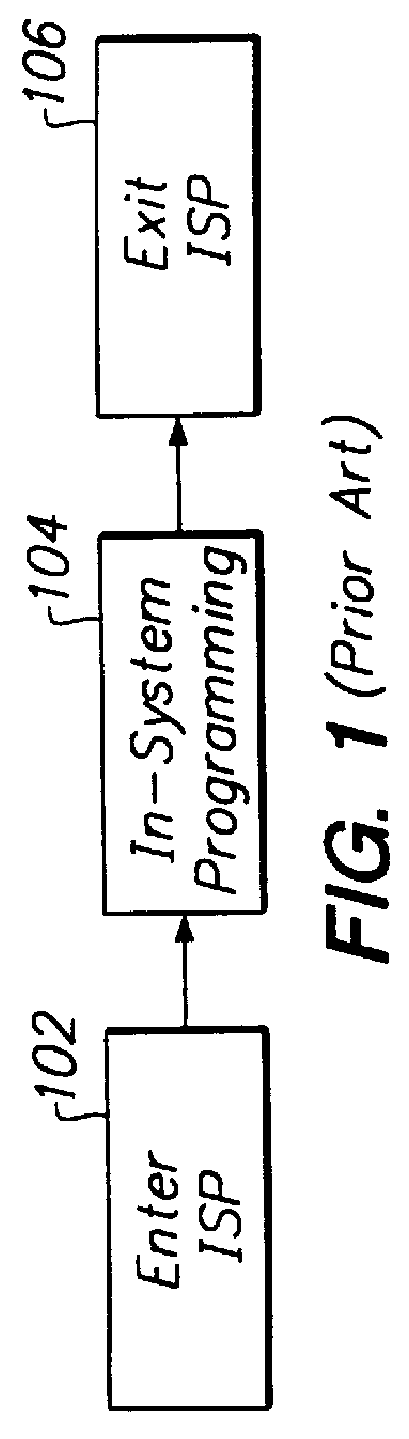
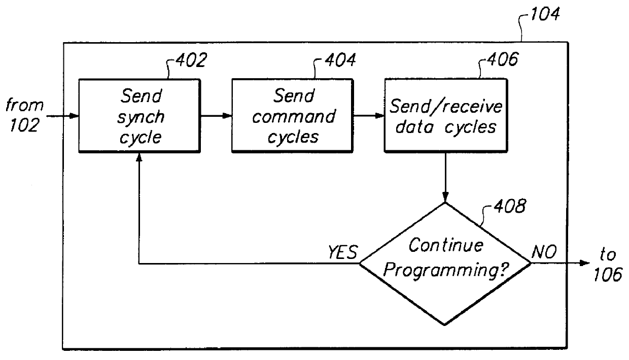
FIG. 1 is a flow diagram showing conventional steps in a general process for in-system programming. The general process includes entering in-system programming mode 102, performing in-system programming 104, and exiting in-system programming mode 106.

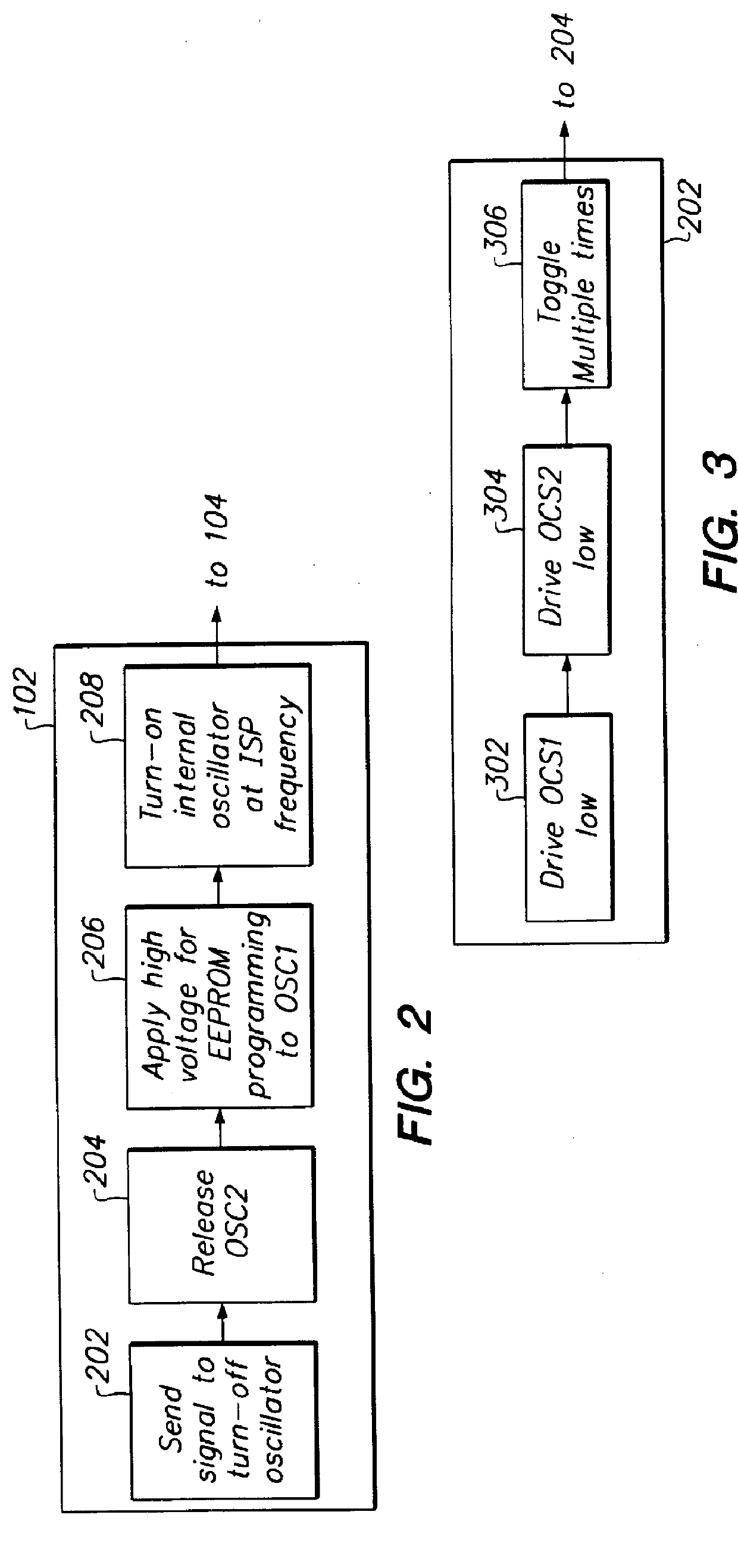
FIG. 2 is a flow diagram showing a method 102 for entering in-system programming mode according to a preferred embodiment of the present invention. The method 102 includes a first step 202 of sending a signal to turn-off an oscillator for the device to be programmed, a second step 204 of releasing a voltage on a second oscillator pin (OSC2), a third step 206 of applying a relatively high voltage to a first oscillator pin (OSC1) to enable EEPROM programming, and a fourth step 208 of tuning-on an oscillator internal to the device to be programmed at a frequency corresponding to in-system programming cycles.

FIG. 3 is a flow diagram showing a method 202 for sending a signal to turn-off an oscillator according to a preferred embodiment of th...


PUM


Abstract

A method and apparatus for In-System Programming which overcomes the above-described disadvantages. The method and apparatus of the ISP system interfaces with the two oscillator (instead of I / O) pins on the microcontroller. By interfacing with the two oscillator pins, the need for extra isolation circuitry to isolate other circuits from the ISP circuits is avoided in most circumstances, without incurring the expense of an expensive JTAG tester or extra dedicated pins. The amount of isolation circuitry necessary is reduced because the two oscillator pins are usually connected to passive components (registers, capacitors, or crystals) which cannot be damaged by the relatively high programming voltages and which do not produce signals that would interfere with the ISP programming signals.

Description

I. BACKGROUND OF THE INVENTIONA. Technical FieldThe present invention relates to programming memory on a semiconductor chip. More particularly, this invention relates to writing data to and reading data from an EEPROM (electrically erasable programmable read-only memory).B. Related Art1. In-System Programming (ISP)An EEPROM is typically programmed by inserting the EEPROM chip into a socket of a PROM programmer machine. The EEPROM is then mounted on a circuit board of a system (i.e. the system board). Subsequently, if it is desired to re-program the EEPROM, then the EEPROM would typically be removed from the system board and re-inserted into the socket of the PROM programmer. This need to remove the EEPROM from the system board in order to re-program the EEPROM is a disadvantage which may slow-down product development, hinder in-field upgrades / bug fixes, and increase the amount of chips that need to be over-stocked in order to facilitate upgrades / bug fixes.In-System Programming (ISP)...

Claims


Application Information

Patent Timeline
Patent Type & Authority Patents(United States)
IPC IPC(8): G11C16/06G11C16/10
CPCG11C16/102
Inventor SZETO, KINYUEGRACEY, CHARLES M.CHENG, CHUCK C.W.
Owner QUALCOMM INC
Why Eureka
Try Eureka