

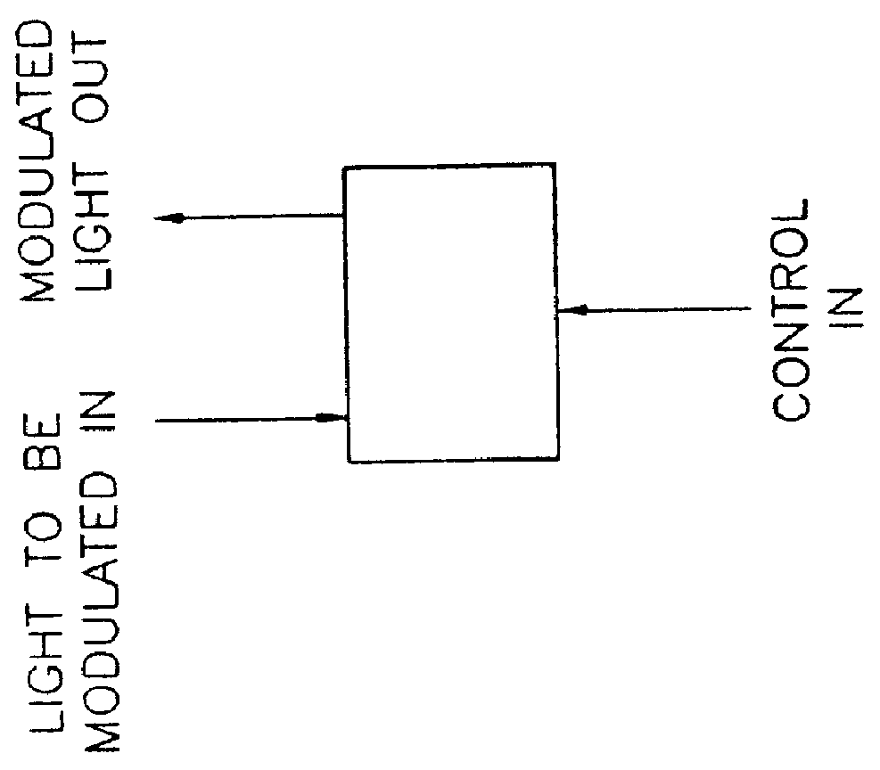
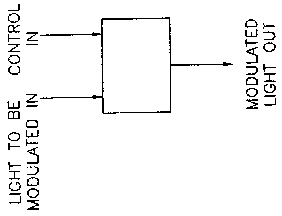
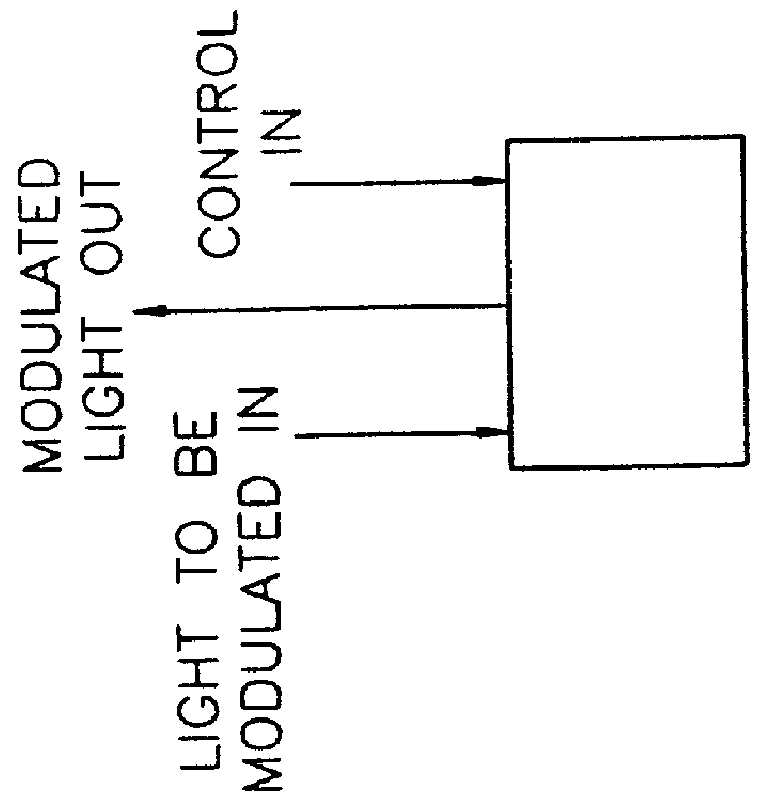
Monolithic all-semiconductor optically addressed spatial light modulator based on low-photoconductive semiconductors
a technology of low-photoconductive semiconductors and all-semiconductor, which is applied in the field of monolithic all-semiconductor optically addressed spatial light modulators based on low-photoconductive semiconductors, can solve the problems of loss of device resolution, loss of device efficiency, and loss of pixel less well defined, and achieve good device resolution and lateral isolation good
- Summary
- Abstract
- Description
- Claims
- Application Information
AI Technical Summary
Benefits of technology
Problems solved by technology
Method used
Image

Examples
example 2
OASLM 200 can be formed as follows. First, conductive substrate 225 and mirror electrode 220 are formed as in Example 1 above.
Next, three sets of the substructure 230 (i.e., buffer layer 210 / electrooptic region 215 / buffer layer 210) are formed. Each set of the substructure 230 comprises a 76 period thick multiple quantum well (MQW) region of 40 angstrom thick Al.sub.0.1 Ga.sub.0.9 As / 50 angstrom thick GaAs, sandwiched between 4000 angstrom thick layers of low temperature growth gallium aluminum arsenide, e.g., Al.sub.0.3 Ga.sub.0.7 As.
In practice, OASLM 200 can be made quite small, e.g., as small as 1-3 micrometers in thickness.
And in practice, OASLM 200 has also proven to be a fast device, providing response times ranging between picoseconds and microseconds, depending on the intensity of the control light.
PUM
| Property | Measurement | Unit |
|---|---|---|
| thickness | aaaaa | aaaaa |
| thickness | aaaaa | aaaaa |
| transparent | aaaaa | aaaaa |
Abstract
Description
Claims
Application Information